

Crystalline silicon
Semiconducting material used in solar cell technology
- 15 min read
- 7 chapters

Related on Lably
Through Crystal, Silicon and Semiconductor
In electronics, crystalline silicon is typically the monocrystalline form of silicon, and is used for producing microchips. This silicon contains much lower impurity levels than those required for solar cells. Production of semiconductor grade silicon involves a chemical purification to produce hyper-pure polysilicon, followed by a recrystallization process to grow monocrystalline silicon. The cylindrical boules are then cut into wafers for further processing.
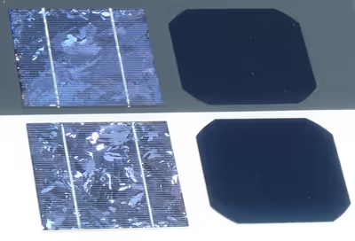
Solar cells made of crystalline silicon are often called conventional, traditional, or first generation solar cells, as they were developed in the 1950s and remained the most common type up to the present time. Because they are produced from 160 to 190 μm thick solar wafers—slices from bulks of solar grade silicon—they are sometimes called wafer-based solar cells.
Solar cells made from c-Si are single-junction cells and are generally more efficient than their rival technologies, which are the second-generation thin-film solar cells, the most important being CdTe, CIGS, and amorphous silicon (a-Si). Amorphous silicon is an allotropic variant of silicon, and amorphous means "without shape" to describe its non-crystalline form.
Overview
Classification
The allotropic forms of silicon range from a single crystalline structure to a completely unordered amorphous structure with several intermediate varieties. In addition, each of these different forms can possess several names and even more abbreviations, and often cause confusion to non-experts, especially as some materials and their application as a PV technology are of minor significance, while other materials are of outstanding importance.
PV industry
In photovoltaic industry, materials are commonly grouped into the following two categories:
- Crystalline silicon (c-Si), used in conventional wafer-based solar cells.
- Monocrystalline silicon (mono-Si)
- Polycrystalline silicon (multi-Si)
- Ribbon silicon (ribbon-Si), has currently no market
- Other materials, not classified as crystalline silicon, used in thin-film and other solar-cell technologies.
- Amorphous silicon (a-Si)
- Nanocrystalline silicon (nc-Si)
- Protocrystalline silicon (pc-Si)
- Other established non-silicon materials, such as CdTe, CIGS
- Emerging photovoltaics
- Multi-junction solar cells (MJ) commonly used for solar panels on spacecraft for space-based solar power. They are also used in concentrator photovoltaics (CPV, HCPV), an emerging technology best suited for locations that receive much sunlight.
Generations
Alternatively, different types of solar cells and/or their semiconducting materials can be classified by generations:
- First-generation solar cells are made of crystalline silicon, also called conventional, traditional, wafer-based solar cells, and include monocrystalline (mono-Si) and polycrystalline (multi-Si) semiconducting materials.
- Second-generation solar cells or panels are based on thin-film technology and are of commercially significant importance. These include CdTe, CIGS, and amorphous silicon.
- Third-generation solar cells are often labeled as emerging technologies with little or no market significance and include a large range of substances, mostly organic, often using organometallic compounds.
Arguably, multi-junction photovoltaic cells can be classified to neither of these generations. A typical triple junction semiconductor is made of InGaP/(In)GaAs/Ge.
Comparison of technical specifications
Market share
In 2013, conventional crystalline silicon technology dominated worldwide PV production, with multi-Si leading the market ahead of mono-Si, accounting for 54% and 36%, respectively. For the last ten years, worldwide market-share of thin-film technologies stagnated below 18% and currently stand at 9%. In the thin-film market, CdTe leads with an annual production of 2 GWp or 5%, followed by a-Si and CIGS, both around 2%. Alltime deployed PV capacity of 139 gigawatts (cumulative as of 2013) splits up into 121 GW crystalline silicon (87%) and 18 GW thin-film (13%) technology.
Efficiency
The conversion efficiency of PV devices describes the energy-ratio of the outgoing electrical power compared to the incoming radiated light. A single solar cells has generally a better, or higher efficiency than an entire solar module. Additionally, lab efficiency is always far superior to that of goods that are sold commercially.
Lab cells
In 2013, record lab cell efficiency was highest for crystalline silicon. However, multi-silicon is followed closely by cadmium telluride and copper indium gallium selenide solar cells.
- 25.6% — mono-Si cell
- 20.4% — multi-Si cell
- 21.7% — CIGS cell
- 21.5% — CdTe cell
Both-sides-contacted silicon solar cells as of 2021: 26% and possibly above.
Modules
The average commercial crystalline silicon module increased its efficiency from about 12% to 16% over the last ten years. In the same period CdTe-modules improved their efficiency from 9 to 16%. The modules performing best under lab conditions in 2014 were made of monocrystalline silicon. They were 7% above the efficiency of commercially produced modules (23% over 16%) which indicated that the conventional silicon technology still had potential to improve and therefore maintain its leading position.
Energy costs of manufacture
Crystalline silicon has a high cost in energy because silicon is produced by the reduction of high-grade quartz sand in an electric furnace. The electricity generated for this process may produce greenhouse gas emissions. This coke-fired smelting process occurs at high temperatures of more than 1,000 °C and is very energy intensive, using about 11 kilowatt-hours (kW⋅h) per kilogram of silicon.
The energy requirements of this process per unit of silicon metal produced may be relatively inelastic. However, significant reductions in energy cost per photovoltaic product have been achieved as silicon cells have become more efficient at converting sunlight, larger silicon ingots are cut with less waste into thinner wafers, silicon waste from manufacturing is recycled, and material costs have declined.
Toxicity
With the exception of amorphous silicon, most commercially established PV technologies use toxic heavy metals. CIGS often uses a CdS buffer layer, and the semiconductor material of CdTe-technology itself contains the toxic cadmium (Cd). In the case of crystalline silicon modules, the solder material that joins the copper strings of the cells, it contains about 36% of lead (Pb). Moreover, the paste used for screen printing front and back contacts contains traces of Pb and sometimes Cd as well. It is estimated that about 1,000 metric tonnes of Pb have been used for 100 gigawatts of c-Si solar modules. However, there is no fundamental need for lead in the solder alloy.
Sign in to keep reading
6 more chapters are free with a Lably account.
Properties
Crystalline silicon has become large in the semiconductor and solar spaces, primarily for its electronic properties, specifically its moderate valence band and high charge carrier mobility. But it is the mechanical properties of crystalline silicon wafers that have allowed this material to become scaled and commercialized, and mechanical and electronic properties go hand in hand. The ease of manufacturing crystalline silicon wafers are also largely owed to their mechanical properties.
The mechanical properties of pure, undoped monocrystalline silicon are included below. Due to its diamond cubic crystal structure, some of these properties are anisotropic depending on the crystallographic orientation along which they are measured, or depending upon the crystallographic plane along which the wafers are cut.
These mechanical properties are relevant both for the semiconductor industry, where silicon substrates are used as circuit supports, and for the PV industry, where silicon solar panels are often exposed to extreme weather conditions. In both cases, however, crystalline silicon is typically doped with certain other elements (Group 13 elements for more positive charge carriers, Group 15 elements for more negative charge carriers) to increase conductivity and shift the bandgap, which simultaneously modifies the mechanical properties. It has been shown that increasing dopant concentration can decrease the shear modulus, increase the bulk modulus, decrease the stiffness (elastic modulus), and shift the material from the brittle to the ductile regime. This results in overall increased toughness, which is useful for manufacturing, and increased elasticity and ductility.
In the PV industry, recent demand has risen for flexible solar cells that can be mounted on a variety of uneven or mobile surfaces and integrated into existing structures. While it is a relatively mature technology, crystalline silicon solar has maintained its lead as the most widespread and most efficient solar technology on the market, so researchers have long sought to adapt the technology to make it flexible and lightweight. This goal has remained elusive because it is a major challenge due to the inherent brittleness of crystalline silicon. In a new landmark study, researchers from China developed a method to create flexible crystalline silicon wafers. When crystalline silicon wafers are cut, the surface of these wafers are typically textured/micropatterned to increase the surface area and allow for better light absorption. This technique creates lots of sharp valleys at which cracks easily form when the wafer is bent, ultimately leading to brittle fractures. As a solution to this problem, the researchers blunted the tips at the edges of the wafer, eliminating the source of fractures and ultimately creating crystalline silicon solar cells that maintain their power conversion efficiency throughout bending cycles.
Cell technologies
PERC solar cell
Passivated emitter rear contact (PERC) solar cells consist of the addition of an extra layer to the rear-side of a solar cell. This dielectric passive layer acts to reflect unabsorbed light back to the solar cell for a second absorption attempt increasing the solar cell efficiency.
A PERC is created through an additional film deposition and etching process. Etching can be done either by chemical or laser processing. About 80% of solar panels worldwide use the PERC design. Martin Green, Andrew Blakers, Jianhua Zhao and Aihua Wang won the Queen Elizabeth Prize for Engineering in 2023 for development of the PERC solar cell.
HIT solar cell
A HIT solar cell is composed of a mono thin crystalline silicon wafer surrounded by ultra-thin amorphous silicon layers. The acronym HIT stands for "heterojunction with intrinsic thin layer". HIT cells are produced by the Japanese multinational electronics corporation Panasonic (see also Sanyo § Solar cells and plants). Panasonic and several other groups have reported several advantages of the HIT design over its traditional c-Si counterpart:
- An intrinsic a-Si layer can act as an effective surface passivation layer for c-Si wafer.
- The p+/n+ doped a-Si functions as an effective emitter/BSF for the cell.
- The a-Si layers are deposited at much lower temperature, compared to the processing temperatures for traditional diffused c-Si technology.
- The HIT cell has a lower temperature coefficient compared to c-Si cell technology.
Owing to all these advantages, this new hetero-junction solar cell is a considered to be a promising low cost alternative to traditional c-Si based solar cells.
Fabrication of HIT cells
The details of the fabrication sequence vary from group to group. Typically in good quality, CZ/FZ grown c-Si wafer (with ~1 ms lifetimes) are used as the absorber layer of HIT cells. Using alkaline etchants, such as, NaOH or (CH3)4NOH the (100) surface of the wafer is textured to form the pyramids of 5–10 μm height. Next, the wafer is cleaned using peroxide and HF solutions. This is followed by deposition of intrinsic a-Si passivation layer, typically through PECVD or Hot-wire CVD. The silane (SiH4) gas diluted with H2 is used as a precursor. The deposition temperature and pressure is maintained at 200 °C and 0.1−1 Torr. Precise control over this step is essential to avoid the formation of defective epitaxial Si.
Cycles of deposition and annealing and H2 plasma treatment are shown to have provided excellent surface passivation. Diborane or Trimethylboron gas mixed with SiH4 is used to deposit p-type a-Si layer, while, Phosphine gas mixed with SiH4 is used to deposit n-type a-Si layer. Direct deposition of doped a-Si layers on c-Si wafer is shown to have very poor passivation properties. This is most likely due to dopant induced defect generation in a-Si layers. Sputtered Indium Tin Oxide (ITO) is commonly used as a transparent conductive oxide (TCO) layer on top of the front and back a-Si layer in bi-facial design, as a-Si has high lateral resistance.
It is generally deposited on the back side as well fully metallized cell to avoid diffusion of back metal and also for impedance matching for the reflected light. The silver/aluminum grid of 50-100μm thick is deposited through stencil printing for the front contact and back contact for bi-facial design. The detailed description of the fabrication process can be found in.
Opto-electrical modeling and characterization of HIT cells
The literature discusses several studies to interpret carrier transport bottlenecks in these cells. Traditional light and dark I–V are extensively studied and are observed to have several non-trivial features, which cannot be explained using the traditional solar cell diode theory. This is because of the presence of hetero-junction between the intrinsic a-Si layer and c-Si wafer which introduces additional complexities to current flow. In addition, there has been significant efforts to characterize this solar cell using C-V, impedance spectroscopy, surface photo-voltage, suns-Voc to produce complementary information.
Further, a number of design improvements, such as, the use of new emitters, bifacial configuration, interdigitated back contact (IBC) configuration bifacial-tandem configuration are actively being pursued.
Mono-silicon
Monocrystalline silicon (mono c-Si) is a form in which the crystal structure is homogeneous throughout the material; the orientation, lattice parameter, and electronic properties are constant throughout the material. Dopant atoms such as phosphorus and boron are often incorporated into the film to make the silicon n-type or p-type respectively. Monocrystalline silicon is fabricated in the form of silicon wafers, usually by the Czochralski Growth method, and can be quite expensive depending on the radial size of the desired single crystal wafer (around $200 for a 300 mm Si wafer). This monocrystalline material, while useful, is one of the chief expenses associated with producing photovoltaics where approximately 40% of the final price of the product is attributable to the cost of the starting silicon wafer used in cell fabrication.
Polycrystalline silicon
Polycrystalline silicon is composed of many smaller silicon grains of varied crystallographic orientation, typically > 1 mm in size. This material can be synthesized easily by allowing liquid silicon to cool using a seed crystal of the desired crystal structure. Additionally, other methods for forming smaller-grained polycrystalline silicon (poly-Si) exist such as high temperature chemical vapor deposition (CVD).
Not classified as Crystalline silicon
These allotropic forms of silicon are not classified as crystalline silicon. They belong to the group of thin-film solar cells.
Amorphous silicon
Amorphous silicon (a-Si) has no long-range periodic order. The application of amorphous silicon to photovoltaics as a standalone material is somewhat limited by its inferior electronic properties. When paired with microcrystalline silicon in tandem and triple-junction solar cells, however, higher efficiency can be attained than with single-junction solar cells. This tandem assembly of solar cells allows one to obtain a thin-film material with a bandgap of around 1.12 eV (the same as single-crystal silicon) compared to the bandgap of amorphous silicon of 1.7–1.8 eV bandgap. Tandem solar cells are then attractive since they can be fabricated with a bandgap similar to single-crystal silicon but with the ease of amorphous silicon.
Nanocrystalline silicon
Nanocrystalline silicon (nc-Si), sometimes also known as microcrystalline silicon (μc-Si), is a form of porous silicon. It is an allotropic form of silicon with paracrystalline structure—is similar to amorphous silicon (a-Si), in that it has an amorphous phase. Where they differ, however, is that nc-Si has small grains of crystalline silicon within the amorphous phase. This is in contrast to polycrystalline silicon (poly-Si) which consists solely of crystalline silicon grains, separated by grain boundaries. The difference comes solely from the grain size of the crystalline grains. Most materials with grains in the micrometre range are actually fine-grained polysilicon, so nanocrystalline silicon is a better term. The term 'nanocrystalline silicon' refers to a range of materials around the transition region from amorphous to microcrystalline phase in the silicon thin film.
Protocrystalline silicon
Protocrystalline silicon has a higher efficiency than amorphous silicon (a-Si) and it has also been shown to improve stability, but not eliminate it. A Protocrystalline phase is a distinct phase occurring during crystal growth which evolves into a microcrystalline form.
Protocrystalline Si also has a relatively low absorption near the band gap owing to its more ordered crystalline structure. Thus, protocrystalline and amorphous silicon can be combined in a tandem solar cell where the top layer of thin protocrystalline silicon absorbs short-wavelength light whereas the longer wavelengths are absorbed by the underlying a-Si substrate.
Transformation of amorphous into crystalline silicon
Amorphous silicon can be transformed to crystalline silicon using well-understood and widely implemented high-temperature annealing processes. The typical method used in industry requires high-temperature compatible materials, such as special high temperature glass that is expensive to produce. However, there are many applications for which this is an inherently unattractive production method.
Low temperature induced crystallization
Flexible solar cells have been a topic of interest for less conspicuous-integrated power generation than solar power farms. These modules may be placed in areas where traditional cells would not be feasible, such as wrapped around a telephone pole or cell phone tower. In this application, a photovoltaic material may be applied to a flexible substrate, often a polymer. Such substrates cannot survive the high temperatures experienced during traditional annealing. Instead, novel methods of crystallizing the silicon without disturbing the underlying substrate have been studied extensively. Aluminum-induced crystallization (AIC) and local laser crystallization are common in the literature, however not extensively used in industry.
In both of these methods, amorphous silicon is grown using traditional techniques such as plasma-enhanced chemical vapor deposition (PECVD). The crystallization methods diverge during post-deposition processing. In aluminum-induced crystallization, a thin layer of aluminum (50 nm or less) is deposited by physical vapor deposition onto the surface of the amorphous silicon. This stack of material is then annealed at a relatively low temperature between 140 °C and 200 °C in a vacuum. The aluminum that diffuses into the amorphous silicon is believed to weaken the hydrogen bonds present, allowing crystal nucleation and growth. Experiments have shown that polycrystalline silicon with grains on the order of 0.2–0.3 μm can be produced at temperatures as low as 150 °C. The volume fraction of the film that is crystallized is dependent on the length of the annealing process.
Aluminum-induced crystallization produces polycrystalline silicon with suitable crystallographic and electronic properties that make it a candidate for producing polycrystalline thin films for photovoltaics. AIC can be used to generate crystalline silicon nanowires and other nano-scale structures.
Another method of achieving the same result is the use of a laser to heat the silicon locally without heating the underlying substrate beyond some upper-temperature limit. An excimer laser or, alternatively, green lasers such as a frequency-doubled Nd:YAG laser is used to heat the amorphous silicon, supplying the energy necessary to nucleate grain growth. The laser fluence must be carefully controlled in order to induce crystallization without causing widespread melting. Crystallization of the film occurs as a very small portion of the silicon film is melted and allowed to cool. Ideally, the laser should melt the silicon film through its entire thickness, but not damage the substrate. Toward this end, a layer of silicon dioxide is sometimes added to act as a thermal barrier. This allows the use of substrates that cannot be exposed to the high temperatures of standard annealing, polymers for instance. Polymer-backed solar cells are of interest for seamlessly integrated power production schemes that involve placing photovoltaics on everyday surfaces.
A third method for crystallizing amorphous silicon is the use of a thermal plasma jet. This strategy is an attempt to alleviate some of the problems associated with laser processing – namely the small region of crystallization and the high cost of the process on a production scale. The plasma torch is a simple piece of equipment that is used to anneal the amorphous silicon thermally. Compared to the laser method, this technique is simpler and more cost-effective. Plasma torch annealing is attractive because the process parameters and equipment dimensions can be changed easily to yield varying levels of performance. A high level of crystallization (~ 90%) can be obtained with this method. Disadvantages include difficulty achieving uniformity in the crystallization of the film. While this method is applied frequently to silicon on a glass substrate, processing temperatures may be too high for polymers.