


Related on Lably
Through Pixel and Catenation
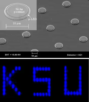
μLED technology was first invented in 2000 by the research group of Hongxing Jiang and Jingyu Lin of Texas Tech University while they were at Kansas State University. The first high-resolution and video-capable InGaN MicroLED display was realized in 2009 by Jiang, Lin and their colleagues via active driving of a microLED array by a complementary metal-oxide semiconductor (CMOS) IC.
MicroLED is an emerging technology and the market is expected to grow in the coming years. The technology is mostly tipped practically for wearables, such as smartwatches, but MicroLED's capability of high speed modulation has proposed it for chip-to-chip interconnect applications as well. Large commercial screens utilizing the technology started being offered in the late 2010s and the first MicroLED televisions for consumers were released in 2021, although manufacturing these displays still remains very expensive.
Research
Following the first report of electrical injection microLEDs based on indium gallium nitride (InGaN) semiconductors in 2000 by the research group of Hongxing Jiang and Jingyu Lin, several groups have quickly engaged in pursuing this concept. Many related potential applications have been identified. Various on-chip connection schemes of microLED pixel arrays have been employed by AC LED Lighting, LLC (a company funded by Jiang and Lin) allowing for the development of single-chip high voltage DC/AC-LEDs to address the compatibility issue between the high voltage electrical infrastructure and low voltage operation nature of LEDs and high brightness self-emissive microdisplays.
The microLED array has also been explored as a light source for optogenetic applications and for visible light communications.
Early InGaN based microLED arrays and microdisplays were primarily passively driven. The first actively driven video-capable self-emissive InGaN microLED microdisplay in VGA format (640 × 480 pixels, each 12 μm in size with 15 μm between them) possessing low voltage requirements was patented and realized in 2009 by Jiang, Lin and their colleagues at Texas Tech and III-N Technology, Inc.(a company funded by Jiang and Lin) via integration between microLED array and CMOS integrated circuit (IC) and the work was also published in the following years.
The first microLED products were demonstrated by Sony in 2012. These displays, however, were very expensive.
There are several methods to manufacture microLED displays. The flip-chip method manufactures the LED on a conventional sapphire substrate, while the transistor array and solder bumps are deposited on silicon wafers using conventional manufacturing and metallization processes. Mass transfer is used to pick and place several thousand LEDs from one wafer to another at the same time, and the LEDs are bonded to the silicon substrate using reflow ovens. The flip-chip method is used for micro displays used on virtual reality headsets. Another microLED manufacturing method involves bonding the LEDs to an IC layer on a silicon substrate and then removing the LED bonding material using conventional semiconductor manufacturing techniques. The current bottleneck in the manufacturing process is the need to individually test every LED and replace faulty ones using an excimer laser lift-off apparatus, which uses a laser to weaken the bond between the LED and its substrate. Faulty LED replacement must be performed using high accuracy pick-and-place machines and the test and repair process takes several hours. The mass transfer process alone can take 18 days, for a smartphone screen with a glass substrate. Special LED manufacturing techniques can be used to increase yield and reduce the amount of faulty LEDs that need to be replaced. Each LED can be as small as 5 μm across. LED epitaxy techniques need to be improved to increase LED yields.
Excimer lasers are used for several steps: laser lift-off to separate LEDs from their sapphire substrate and to remove faulty LEDs, for manufacturing the LTPS-TFT backplane, and for laser cutting of the finished LEDs. Special mass transfer techniques using elastomer stamps are also being researched. Other companies are exploring the possibility of packaging 3 LEDs: one red, one green and one blue LED into a single package to reduce mass transfer costs.
Quantum dots are being researched as a way to shrink the size of microLED pixels, while other companies are exploring the use of phosphors and quantum dots to eliminate the need for different-colored LEDs. Sensors can be embedded in microLED displays.
Over 130 companies are involved in microLED research and development. MicroLED light panels are also being made, and are an alternative to conventional OLED and LED light panels.
Digital pulse-width modulation is well-suited to driving microLED displays. MicroLEDs experience a color shift as the current magnitude changes. Analog schemes change current to change brightness. With a digital pulse, only one current value is used for the on state. Thus, there is no color shift that occurs as brightness changes.
Current microLED display offerings by Samsung and Sony consist of "cabinets" that can be tiled to create a large display of any size, with the display's resolution increasing with size. They also contain mechanisms to protect the display against water and dust. Each cabinet is 36.4 inches (92 cm) diagonally with a resolution of 960 × 540.
Sign in to keep reading
One more chapter is free with a Lably account.
Commercialization
Television
MicroLEDs have already demonstrated performance advantages over LCD and OLED displays, including higher brightness, lower latency, higher contrast ratio, greater color saturation, intrinsic self-illumination, better efficiency and longer lifetime. Compared with OLED displays and LCDs, microLED displays stand out for their combination of high performance, durability, and energy efficiency. Ultrahigh brightness is particularly relevant for applications in augmented-reality displays that compete with the Sun's brightness in outdoor environments.
Glo and Jasper Display Corporation demonstrated the world's first RGB microLED microdisplay, measuring 0.55 inches (1.4 cm) diagonally, at SID Display Week 2017. Glo transferred their microLEDs to the Jasper Display backplane.
Sony launched a 55-inch (140 cm) "Crystal LED Display" in 2012 with 1920 × 1080 resolution, as a demonstration product. Sony announced its CLEDIS (Crystal LED Integrated Structure) brand which used surface mounted LEDs for large display production. As of August 2019, Sony offers CLEDIS in 146-inch (3.7 m), 182-inch (4.6 m) and 219-inch (5.6 m) displays. On 12 September 2019, Sony announced Crystal LED availability to consumers ranging from 1080p 110-inch (2.8 m) to 16K 790-inch (20 m) displays.
Samsung demonstrated a 146-inch (3.7 m) microLED display called The Wall at CES 2018. In July 2018, Samsung announced plans on bringing a 4K microLED TV to consumer market in 2019. At CES 2019, Samsung demonstrated a 75-inch (1.9 m) 4K microLED display and 219-inch (5.6 m) 6K microLED display. On June 12 at InfoComm 2019, Samsung announced the global launch of The Wall Luxury microLED display configurable from 73-inch (1.9 m) in 2K to 292-inch (7.4 m) in 8K. On October 4, 2019, Samsung announced that The Wall Luxury microLED display shipments had begun.
In March 2018, Bloomberg reported Apple to have about 300 engineers devoted to in-house development of microLED screens. At IFA 2018 in August, LG Display demonstrated a 173-inch (4.4 m) microLED display.
At SID's Display Week 2019 in May, Tianma and PlayNitride demonstrated their co-developed 7.56-inch (19.2 cm) microLED display with over 60% transparency. China Star Optoelectronics Technology (CSoT) demonstrated a 3.3-inch (8.4 cm) transparent microLED display with around 45% transparency, also co-developed with PlayNitride. Plessey Semiconductors Ltd demonstrated a monolithic monochrome blue GaN-on-silicon wafer bonded to a Jasper Display CMOS backplane 0.7-inch (18 mm) active-matrix microLED display with an 8 μm pixel pitch.
At SID's Display Week 2019 in May, Jade Bird Display demonstrated their 720p and 1080p microLED microdisplays with 5 μm and 2.5 μm pitch respectively, achieving luminance in the millions of candelas per square metre. In 2021, Jade Bird Display and Vuzix have entered a Joint manufacturing agreement for making microLED based projectors for smart glasses and augmented reality glasses
At Touch Taiwan 2019 on September 4, 2019, AU Optronics demonstrated a 12.1-inch (31 cm) microLED display and indicated that microLED was 1–2 years from mass commercialization. At IFA 2019 on September 13, 2019, TCL Corporation demonstrated their Cinema Wall featuring a 4K 132-inch (3.4 m) microLED display with maximum brightness of 1,500 cd/m2 and 2,500,000∶1 contrast ratio produced by their subsidiary China Star Optoelectronics Technology (CSoT).
As of 2021, Sony, Samsung, and Konka started to sell microLED video walls. LG, Tianma, PlayNitride, TCL/CSoT, Jasper Display, Jade Bird Display, Plessey Semiconductors Ltd, and Ostendo Technologies, Inc. have demonstrated prototypes. Sony already sells microLED displays as a replacement for conventional cinema screens. BOE, Epistar, and Leyard have plans for microLED mass production. MicroLED can be made flexible and transparent, just like OLEDs.
According to a report by Market Research Future, the MicroLED display market will reach around USD 24.3 billion by 2027. Custom Market Insights reported that the MicroLED display market is expected to reach around USD 182.7 Billion by 2032.
As of 2024, Samsung has already launched microLED display products including The Wall. Samsung's microLED display technology transfers micrometer-scale LEDs into LED modules, resulting in what resembles wall tiles composed of mass-transferred clusters of almost microscopic lights.
Samsung has also debuted at 2024 CES their Transparent MicroLED display.
LG has also debuted at 2024 CES their microLED display, called LG MAGNIT.
In terms of microLED microdisplay, Jade Bird Display launched 0.13" series of MicroLED displays which has an active area of 0.13" (3.3 mm) in diagonal and a resolution of 640X480 for AR and VR display products.
Apple reportedly invested billions of dollars in development of microLED displays in the years leading up to 2024, intending to transition its products to the technology beginning with the Apple Watch Ultra, before ultimately abandoning the effort after deciding it was unviable. However, the company is reportedly still "eyeing microLED for other projects down the road".
Optical interconnects
MicroLEDs can be densely arranged in an array and coupled onto fiber-optic cable to transmit information at up to 1 Tb/s while keeping power consumption and bit error rate lower than traditionally used laser diodes or silicon photonics.