

Field-programmable gate array
Array of logic gates that are reprogrammable
- 19 min read
- 7 chapters

Related on Lably
Through Circuit diagram, Logic gate and AND gate
An FPGA configuration is generally written using a hardware description language (HDL), e.g., VHDL, similar to the ones used for application-specific integrated circuits (ASICs). Circuit diagrams were formerly used to write the configuration.
The logic blocks of an FPGA can be configured to perform complex combinational functions, or act as simple logic gates like AND and XOR. In most FPGAs, logic blocks also include memory elements, which may be simple flip-flops or more sophisticated blocks of memory. Many FPGAs can be reprogrammed to implement different logic functions, allowing flexible reconfigurable computing as performed in computer software.
FPGAs also have a role in embedded system development due to their capability to start system software development simultaneously with hardware, enable system performance simulations at a very early phase of the development, and allow various system trials and design iterations before finalizing the system architecture.
FPGAs are also commonly used during the development of ASICs to speed up the simulation process.
History
The FPGA industry sprouted from programmable read-only memory (PROM) and programmable logic devices (PLDs). PROMs and PLDs both had the option of being programmed in batches in a factory or in the field (field-programmable).
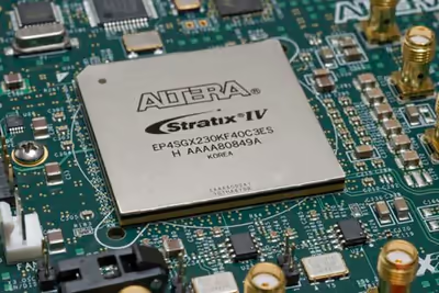
Altera was founded in 1983 and delivered the industry's first reprogrammable logic device in 1984 – the EP300 – which featured a quartz window in the package that allowed users to shine an ultraviolet lamp on the die to erase the EPROM cells that held the device configuration.
Xilinx (now owned by AMD) produced the first commercially viable field-programmable gate array in 1985 – the XC2064. The XC2064 had programmable gates and programmable interconnects between gates, the beginnings of a new technology and market. The XC2064 had 64 configurable logic blocks (CLBs), with two three-input lookup tables (LUTs).
In 1987, the Naval Surface Warfare Center funded an experiment proposed by Steve Casselman to develop a computer that would implement 600,000 reprogrammable gates. Casselman was successful and a patent related to the system was issued in 1992.
Altera and Xilinx continued unchallenged and quickly grew from 1985 to the mid-1990s when competitors sprouted up, eroding a significant portion of their market share. By 1993, Actel (later Microsemi, now Microchip) was serving about 18 percent of the market.
The 1990s were a period of rapid growth for FPGAs, both in circuit sophistication and the volume of production. In the early 1990s, FPGAs were primarily used in telecommunications and networking. By the end of the decade, FPGAs found their way into consumer, automotive, and industrial applications.
By 2013, Altera (31 percent), Xilinx (36 percent), and Actel (10 percent) together represented approximately 77 percent of the FPGA market.
Companies like Microsoft have started to use FPGAs to accelerate high-performance, computationally intensive systems (like the data centers that operate their Bing search engine), due to the performance per watt advantage FPGAs deliver. Microsoft began using FPGAs to accelerate Bing in 2014, and in 2018 began deploying FPGAs across other data center workloads for their Azure cloud computing platform.
Since 2019, modern generations of FPGAs have been integrated with other architectures like AI engines to target workloads in the artificial intelligence domain.
Growth
The following timelines indicate progress in different aspects of FPGA design.
Gates
- 1987: 9,000 gates, Xilinx
- 1992: 600,000, Naval Surface Warfare Department
- Early 2000s: millions
- 2013: 50 million, Xilinx
Market size
- 1985: First commercial FPGA : Xilinx XC2064
- 1987: $14 million
- c. 1993: >$385 million
- 2005: $1.9 billion
- 2010 estimates: $2.75 billion
- 2013: $5.4 billion
- 2020 estimate: $9.8 billion
- 2030 estimate: $23.34 billion
Design starts
A design start is a new custom design for implementation on an FPGA.
- 2005: 80,000
- 2008: 90,000
Sign in to keep reading
6 more chapters are free with a Lably account.
Design
Contemporary FPGAs have ample logic gates and RAM blocks to implement complex digital computations. FPGAs can be used to implement any logical function that an ASIC can perform. The ability to update the functionality after shipping, partial re-configuration of a portion of the design and the low non-recurring engineering costs relative to an ASIC design (notwithstanding the generally higher unit cost), offer advantages for many applications.
As FPGA designs employ very fast I/O rates and bidirectional data buses, it becomes a challenge to verify correct timing of valid data within setup time and hold time. Floor planning helps resource allocation within FPGAs to meet these timing constraints.
Some FPGAs have analog features in addition to digital functions. The most common analog feature is a programmable slew rate on each output pin. This allows the user to set low rates on lightly loaded pins that would otherwise ring or couple unacceptably, and to set higher rates on heavily loaded high-speed channels that would otherwise run too slowly. Also common are quartz-crystal oscillator driver circuitry, on-chip RC oscillators, and phase-locked loops with embedded voltage-controlled oscillators used for clock generation and management as well as for high-speed serializer and deserializer (SERDES) transmit clocks and receiver clock recovery. Fairly common are differential comparators on input pins designed to be connected to differential signaling channels. A few mixed-signal FPGAs have integrated peripheral analog-to-digital converters (ADCs) and digital-to-analog converters (DACs) with analog signal conditioning blocks, allowing them to operate as a system on a chip (SoC). Such devices blur the line between an FPGA, which carries digital ones and zeros on its internal programmable interconnect fabric, and field-programmable analog array (FPAA), which carries analog values on its internal programmable interconnect fabric.
Logic blocks
The most common FPGA architecture consists of an array of logic blocks called configurable logic blocks (CLBs) or logic array blocks (LABs) (depending on vendor), I/O pads, and routing channels. Generally, all the routing channels have the same width (number of signals). Multiple I/O pads may fit into the height of one row or the width of one column in the array.
"An application circuit must be mapped into an FPGA with adequate resources. While the number of logic blocks and I/Os required is easily determined from the design, the number of routing channels needed may vary considerably even among designs with the same amount of logic. For example, a crossbar switch requires much more routing than a systolic array with the same gate count. Since unused routing channels increase the cost (and decrease the performance) of the FPGA without providing any benefit, FPGA manufacturers try to provide just enough channels so that most designs that will fit in terms of lookup tables (LUTs) and I/Os can be routed. This is determined by estimates such as those derived from Rent's rule or by experiments with existing designs."
In general, a logic block consists of a few logical cells. A typical cell consists of a 4-input LUT, a full adder (FA) and a D-type flip-flop. The LUT might be split into two 3-input LUTs. In normal mode those are combined into a 4-input LUT through the first multiplexer (mux). In arithmetic mode, their outputs are fed to the adder. The selection of mode is programmed into the second mux. The output can be either synchronous or asynchronous, depending on the programming of the third mux. In practice, the entire adder or parts of it are stored as functions into the LUTs in order to save space.
Hard blocks
Modern FPGA families expand upon the above capabilities to include higher-level functionality fixed in silicon. Having these common functions embedded in the circuit reduces the area required and gives those functions increased performance compared to building them from logical primitives. Examples of these include multipliers, generic DSP blocks, embedded processors, high-speed I/O logic and embedded memories.
Higher-end FPGAs can contain high-speed multi-gigabit transceivers and hard IP cores such as processor cores, Ethernet medium access control units, PCI or PCI Express controllers, and external memory controllers. These cores exist alongside the programmable fabric, but they are built out of transistors instead of LUTs so they have ASIC-level performance and power consumption without consuming a significant amount of fabric resources, leaving more of the fabric free for the application-specific logic. The multi-gigabit transceivers also contain high-performance signal conditioning circuitry along with high-speed serializers and deserializers, components that cannot be built out of LUTs. Higher-level physical layer (PHY) functionality such as line coding may or may not be implemented alongside the serializers and deserializers in hard logic, depending on the FPGA.
Soft core
An alternate approach to using hard macro processors is to make use of soft processor IP cores that are implemented within the FPGA logic. Nios II, MicroBlaze and Mico32 are examples of popular softcore processors. Many modern FPGAs are programmed at run time, which has led to the idea of reconfigurable computing or reconfigurable systems – CPUs that reconfigure themselves to suit the task at hand. Additionally, new non-FPGA architectures are beginning to emerge. Software-configurable microprocessors such as the Stretch S5000 adopt a hybrid approach by providing an array of processor cores and FPGA-like programmable cores on the same chip.
Integration
In 2012 the coarse-grained architectural approach was taken a step further by combining the logic blocks and interconnects of traditional FPGAs with embedded microprocessors and related peripherals to form a complete system on a programmable chip. Examples of such hybrid technologies can be found in the Xilinx Zynq-7000 all programmable SoC, which includes a 1.0 GHz dual-core ARM Cortex-A9 MPCore processor embedded within the FPGA's logic fabric, or in the Altera Arria V FPGA, which includes an 800 MHz dual-core ARM Cortex-A9 MPCore. The Atmel FPSLIC is another such device, which uses an AVR processor in combination with Atmel's programmable logic architecture. The Microsemi SmartFusion devices incorporate an ARM Cortex-M3 hard processor core (with up to 512 kB of flash and 64 kB of RAM) and analog peripherals such as a multi-channel analog-to-digital converters and digital-to-analog converters in their flash memory-based FPGA fabric.
Clocking
Most of the logic inside of an FPGA is synchronous circuitry that requires a clock signal. FPGAs contain dedicated global and regional routing networks for clock and reset, typically implemented as an H tree, so they can be delivered with minimal skew. FPGAs may contain analog phase-locked loop or delay-locked loop components to synthesize new clock frequencies and manage jitter. Complex designs can use multiple clocks with different frequency and phase relationships, each forming separate clock domains. These clock signals can be generated locally by an oscillator or they can be recovered from a data stream. Care must be taken when building clock domain crossing circuitry to avoid metastability. Some FPGAs contain dual port RAM blocks that are capable of working with different clocks, aiding in the construction of building FIFOs and dual port buffers that bridge clock domains.
3D architectures
To shrink the size and power consumption of FPGAs, vendors such as Tabula and Xilinx have introduced 3D or stacked architectures. Following the introduction of its 28 nm 7-series FPGAs, Xilinx said that several of the highest-density parts in those FPGA product lines will be constructed using multiple dies in one package, employing technology developed for 3D construction and stacked-die assemblies.
Xilinx's approach stacks several (three or four) active FPGA dies side by side on a silicon interposer – a single piece of silicon that carries passive interconnect. The multi-die construction also allows different parts of the FPGA to be created with different process technologies, as the process requirements are different between the FPGA fabric itself and the very high speed 28 Gbit/s serial transceivers. An FPGA built in this way is called a heterogeneous FPGA.
Altera's heterogeneous approach involves using a single monolithic FPGA die and connecting other dies and technologies to the FPGA using Intel's embedded multi-die interconnect bridge (EMIB) technology.
Programming
To define the behavior of the FPGA, the user provides a design in a hardware description language (HDL) or as a schematic design. The HDL form is more suited to work with large structures because it's possible to specify high-level functional behavior rather than drawing every piece by hand. However, schematic entry can allow for easier visualization of a design and its component modules.
Using an electronic design automation tool, a technology-mapped netlist is generated. The netlist can then be fit to the actual FPGA architecture using a process called place and route, usually performed by the FPGA company's proprietary place-and-route software. The user will validate the results using timing analysis, simulation, and other verification and validation techniques. Once the design and validation process is complete, the binary file generated, typically using the FPGA vendor's proprietary software, is used to (re-)configure the FPGA. This file is transferred to the FPGA via a serial interface (JTAG) or to an external memory device such as an EEPROM.
The most common HDLs are VHDL and Verilog. National Instruments' LabVIEW graphical programming language (sometimes referred to as G) has an FPGA add-in module available to target and program FPGA hardware. Verilog was created to simplify the process, making HDL more robust and flexible. Verilog has a C-like syntax, unlike VHDL which is based on Ada.
To simplify the design of complex systems in FPGAs, there exist libraries of predefined complex functions and circuits that have been tested and optimized to speed up the design process. These predefined circuits are commonly called intellectual property (IP) cores, and are available from FPGA vendors and third-party IP suppliers. They are rarely free, and typically released under proprietary licenses. Other predefined circuits are available from developer communities such as OpenCores (typically released under free and open source licenses such as the GPL, BSD or similar license). Such designs are known as open-source hardware.
In a typical design flow, an FPGA application developer will simulate the design at multiple stages throughout the design process. Initially, the RTL description in VHDL or Verilog is simulated by creating test benches to simulate the system and observe results. Then, after the synthesis engine has mapped the design to a netlist, the netlist is translated to a gate-level description where simulation is repeated to confirm the synthesis proceeded without errors. Finally, the design is laid out in the FPGA at which point propagation delay values can be back-annotated onto the netlist, and the simulation can be run again with these values.
More recently, OpenCL (Open Computing Language) is being used by programmers to take advantage of the performance and power efficiencies that FPGAs provide. OpenCL allows programmers to develop code in the C programming language. For further information, see high-level synthesis and C to HDL.
Most FPGAs rely on an SRAM-based approach to be programmed. These FPGAs are in-system programmable and re-programmable, but require external boot devices. For example, flash memory or EEPROM devices may load contents into internal SRAM that controls routing and logic. The SRAM approach is based on CMOS.
Rarer alternatives to the SRAM approach include:
- Fuse: one-time programmable. Bipolar. Obsolete.
- Antifuse: one-time programmable. CMOS. Examples: Actel SX and Axcelerator families; Quicklogic Eclipse II family.
- PROM: programmable read-only memory technology. One-time programmable because of plastic packaging. Obsolete.
- EPROM: erasable programmable read-only memory technology. One-time programmable but with a window so it can be erased with ultraviolet (UV) light. CMOS. Obsolete.
- EEPROM: electrically erasable programmable read-only memory technology. Can be erased, even in plastic packages. Some, but not all, EEPROM devices can be in-system programmed. CMOS.
- Flash: flash-erase EPROM technology. Can be erased, even in plastic packages. Some, but not all, flash devices can be in-system programmed. Usually, a flash cell is smaller than an equivalent EEPROM cell and is, therefore, less expensive to manufacture. CMOS. Example: Actel ProASIC family.
Manufacturers
In 2016, long-time industry rivals Xilinx (now part of AMD) and Altera were the FPGA market leaders. At that time, they controlled nearly 90 percent of the market.
Both Xilinx and Altera provide proprietary electronic design automation software for Windows and Linux (ISE/Vivado and Quartus) which enables engineers to design, analyze, simulate, and synthesize (compile) their designs.
In March 2010, Tabula announced their FPGA technology that uses time-multiplexed logic and interconnect that claims potential cost savings for high-density applications. On March 24, 2015, Tabula officially shut down.
On June 1, 2015, Intel announced it would acquire Altera for approximately US$16.7 billion and completed the acquisition on December 30, 2015.
On October 27, 2020, AMD announced it would acquire Xilinx and completed the acquisition valued at about US$50 billion in February 2022.
In February 2024 Altera became independent of Intel again.
Other manufacturers include:
- Achronix, manufacturing SRAM based FPGAs with 1.5 GHz fabric speed
- Altium, provides system-on-FPGA hardware-software design environment.
- Cologne Chip, German government-backed designer and producer of FPGAs
- Efinix offers small to medium-sized FPGAs. They combine logic and routing interconnects into a configurable XLR cell.
- GOWIN Semiconductors, manufacturing small and medium-sized SRAM and flash-based FPGAs. They also offer pin-compatible replacements for a few Xilinx, Altera and Lattice products.
- Lattice Semiconductor manufactures low-power SRAM-based FPGAs featuring integrated configuration flash, instant-on and live reconfiguration
- SiliconBlue Technologies provides extremely low-power SRAM-based FPGAs with optional integrated nonvolatile configuration memory; acquired by Lattice in 2011
- Microchip:
- Microsemi (previously Actel), producing antifuse, flash-based, mixed-signal FPGAs; acquired by Microchip in 2018
- Atmel, a second source of some Altera-compatible devices; also FPSLIC mentioned above; acquired by Microchip in 2016
- QuickLogic manufactures ultra-low-power sensor hubs, extremely-low-powered, low-density SRAM-based FPGAs, with display bridges MIPI and RGB inputs; MIPI, RGB and LVDS outputs.
Applications
An FPGA can be used to solve any problem that is computable. FPGAs can be used to implement a soft microprocessor, such as the Xilinx MicroBlaze or Altera Nios II. But their advantage lies in that they are significantly faster for some applications because of their parallel nature and optimality in terms of the number of gates used for certain processes.
FPGAs were originally introduced as competitors to complex programmable logic devices (CPLDs) to implement glue logic for printed circuit boards. As their size, capabilities, and speed increased, FPGAs took over additional functions to the point where some are now marketed as full systems on chips (SoCs). Particularly with the introduction of dedicated multipliers into FPGA architectures in the late 1990s, applications that had traditionally been the sole reserve of digital signal processors (DSPs) began to use FPGAs instead.
The evolution of FPGAs has motivated an increase in the use of these devices, whose architecture allows the development of hardware solutions optimized for complex tasks, such as 3D MRI image segmentation, 3D discrete wavelet transform, tomographic image reconstruction, or PET/MRI systems. The developed solutions can perform intensive computation tasks with parallel processing, are dynamically reprogrammable, and have a low cost, all while meeting the hard real-time requirements associated with medical imaging.
Another trend in the use of FPGAs is hardware acceleration, where one can use the FPGA to accelerate certain parts of an algorithm and share part of the computation between the FPGA and a general-purpose processor. The search engine Bing is noted for adopting FPGA acceleration for its search algorithm in 2014. As of 2018, FPGAs are seeing increased use as AI accelerators including Microsoft's Project Catapult and for accelerating artificial neural networks for machine learning applications.
Originally, FPGAs were reserved for specific vertical applications where the volume of production is small. For these low-volume applications, the premium that companies pay in hardware cost per unit for a programmable chip is more affordable than the development resources spent on creating an ASIC. Often a custom-made chip would be cheaper if made in larger quantities, but FPGAs may be chosen to quickly bring a product to market. New cost and performance dynamics have broadened the range of viable applications.
Other uses for FPGAs include:
- Space (with radiation hardening)
- Hardware security modules
- High-speed financial transactions
- Retrocomputing (e.g. the MARS and MiSTer FPGA projects)
- Large scale integrated digital differential analyzers, a form of an analog computer based on digital computing elements
United States military
FPGAs play a crucial role in modern military communications, especially in systems like the Joint Tactical Radio System (JTRS) and in devices from companies such as Thales and Harris Corporation. Their flexibility and programmability make them ideal for military communications, offering customizable and secure signal processing. In the JTRS, used by the US military, FPGAs provide adaptability and real-time processing, crucial for meeting various communication standards and encryption methods.
Retro gaming
FPGAs are used by the retro gaming community in devices like the ModRetro M64 and Analogue 3D because they offer cycle-accurate hardware recreation rather than software simulation. This eliminates the input lag, audio glitches, and timing errors common in traditional emulators. By physically reconfiguring the chips' internal logic to mimic the original console's circuitry, FPGAs allow games to run almost exactly as they did on the original consoles. In 2025 Commodore released the "99.9% backwards compatible" C=64 Ultimate (original C=64 from 1982), based on FPGA design with added modern features like USB, HDMI, and 128MB DDR-2 memory.
Security
Concerning hardware security, FPGAs have both advantages and disadvantages as compared to ASICs or secure microprocessors. FPGAs' flexibility makes malicious modifications during fabrication a lower risk. Previously, for many FPGAs, the design bitstream was exposed while the FPGA loads it from external memory, typically during powerup. All major FPGA vendors now offer a spectrum of security solutions to designers, such as bitstream encryption and authentication. For example, Altera and Xilinx offer AES encryption (up to 256-bit) for bitstreams stored in an external flash memory. Physical unclonable functions (PUFs) are integrated circuits that have their own unique signatures and can be used to secure FPGAs while taking up very little hardware space.
FPGAs that store their configuration internally in nonvolatile flash memory, such as Microsemi's ProAsic 3 or Lattice's XP2 programmable devices, do not expose the bitstream and do not need encryption. Customers wanting a higher guarantee of tamper resistance can use write-once, antifuse FPGAs from vendors such as Microsemi.
With its Stratix 10 FPGAs and SoCs, Altera introduced a Secure Device Manager and physical unclonable functions to provide high levels of protection against physical attacks.
In 2012, researchers Sergei Skorobogatov and Christopher Woods demonstrated that some FPGAs can be vulnerable to hostile intent. They discovered a critical backdoor vulnerability had been manufactured in silicon as part of the Actel/Microsemi ProAsic 3 making it vulnerable on many levels, such as reprogramming crypto and access keys, accessing unencrypted bitstream, modifying low-level silicon features, and extracting configuration data.
In 2020, a critical vulnerability (named Starbleed) was discovered in all Xilinx 7 series FPGAs that rendered bitstream encryption useless. There is no workaround. Xilinx did not produce a hardware revision. Ultrascale and later devices, already on the market at the time, were not affected.
Similar technologies
Historically, FPGAs have been slower, less energy efficient and generally achieved less functionality than their fixed ASIC counterparts. A study from 2006 showed that designs implemented on FPGAs need on average 40 times as much area, draw 12 times as much dynamic power, and run at one third the speed of corresponding ASIC implementations.
Advantages of FPGAs include the ability to reprogram equipment in the field to fix bugs or make other improvements. Some FPGAs have the capability of partial re-configuration that lets one portion of the device be re-programmed while other portions continue running. Other advantages may include shorter time to market and lower non-recurring engineering costs. Vendors can also take a middle road via FPGA prototyping: developing their prototype hardware on FPGAs, but manufacturing their final version as an ASIC after the design has been committed. This is often also the case with new processor designs.
The primary differences between CPLDs and FPGAs are architectural. A CPLD has a comparatively restrictive structure consisting of one or more programmable sum-of-products logic arrays feeding a relatively small number of clocked registers. As a result, CPLDs are less flexible but have the advantage of more predictable propagation delay. FPGA architectures, on the other hand, are dominated by interconnect. This makes them far more flexible but also far more complex to design for, or at least requiring more complex electronic design automation (EDA) software. Another distinction between FPGAs and CPLDs is one of size, as FPGAs are usually much larger in terms of resources than CPLDs. Typically only FPGAs contain more complex embedded functions such as adders, multipliers, memory, and serializer/deserializers. Another common distinction is that CPLDs contain embedded flash memory to store their configuration, while FPGAs typically store their configuration in SRAM and require external non-volatile memory to initialize it on powerup. When a design requires simple instant-on, CPLDs are generally preferred. Sometimes both CPLDs and FPGAs are used in a single system design. In those designs, CPLDs generally perform glue logic functions.