

Flash memory
Electronic non-volatile computer storage device
- 47 min read
- 11 chapters

Related on Lably
Through Non-volatile memory, Word (computer architecture) and Smartphone
Flash memory, a type of floating-gate memory, was invented by Fujio Masuoka at Toshiba in 1980 and is based on EEPROM technology. Toshiba began marketing flash memory in 1987. EPROMs had to be erased completely before they could be rewritten. NAND flash memory, however, may be erased, written, and read in blocks (or pages), which generally are much smaller than the entire device. NOR flash memory allows a single machine word to be written – to an erased location – or read independently. A flash memory device typically consists of one or more flash memory chips (each holding many flash memory cells), along with a separate flash memory controller chip.
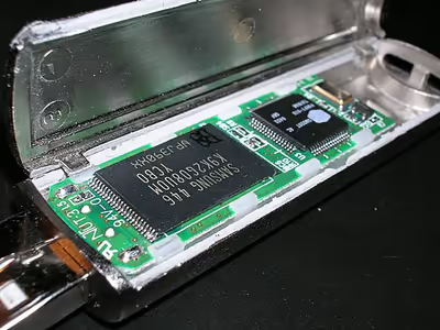
The NAND type is found mainly in memory cards, USB flash drives, solid-state drives (those produced since 2009), feature phones, smartphones, and similar products, for general storage and transfer of data. NAND or NOR flash memory is also often used to store configuration data in digital products, a task previously made possible by EEPROM or battery-powered static RAM. A key disadvantage of flash memory is that it can endure only a relatively small number of write cycles in a specific block.
NOR flash is known for its direct random-access capabilities, making it apt for executing code directly. Its architecture allows for individual byte access, facilitating faster read speeds compared to NAND flash. NAND flash memory operates with a different architecture, relying on a serial access approach. This makes NAND suitable for high-density data storage, but less efficient for random-access tasks. NAND flash is often employed in scenarios where cost-effective, high-capacity storage is crucial, such as in USB drives, memory cards, and solid-state drives (SSDs).
The primary differentiator lies in their use cases and internal structures. NOR flash is optimal for applications requiring quick access to individual bytes, as in embedded systems for program execution. NAND flash, on the other hand, shines in scenarios demanding cost-effective, high-capacity storage with sequential data access.
Flash memory is used in computers, PDAs, digital audio players, digital cameras, mobile phones, synthesizers, video games, scientific instrumentation, industrial robotics, and medical electronics. Flash memory has a fast read access time but is not as fast as static RAM or ROM. In portable devices, it is preferred to use flash memory because of its mechanical shock resistance, since mechanical drives are more prone to mechanical damage.
Because erase cycles are slow, the large block sizes used in flash memory erasing give it a significant speed advantage over non-flash EEPROM when writing large amounts of data. As of 2019, flash memory costs much less than byte-programmable EEPROM and has become the dominant memory type wherever a system required a significant amount of non-volatile solid-state storage. EEPROMs, however, are still used in applications that require only small amounts of storage, e.g. in SPD implementations on computer-memory modules.
Flash memory packages can use die stacking with through-silicon vias and several dozen layers of 3D TLC NAND cells (per die) simultaneously to achieve capacities of up to 1 tebibyte per package using 16 stacked dies and an integrated flash controller as a separate die inside the package.
History
Background
The origins of flash memory can be traced to the development of the floating-gate MOSFET (FGMOS), also known as the floating-gate transistor. The original MOSFET was invented at Bell Labs between 1959 and 1960. Dawon Kahng went on to develop a variation, the floating-gate MOSFET, with Taiwanese-American engineer Simon Min Sze at Bell Labs in 1967. They proposed that it could be used as floating-gate memory cells for storing a form of programmable read-only memory (PROM) that is both non-volatile and re-programmable.
Early types of floating-gate memory included EPROM (erasable PROM) and EEPROM (electrically erasable PROM) in the 1970s. However, early floating-gate memory required engineers to build a memory cell for each bit of data, which proved to be cumbersome, slow, and expensive, restricting floating-gate memory to niche applications in the 1970s, such as military equipment and the earliest experimental mobile phones.
Modern EEPROM based on Fowler-Nordheim tunnelling to erase data was invented by Bernward and patented by Siemens in 1974. It was further developed between 1976 and 1978 by Eliyahou Harari at Hughes Aircraft Company, as well as by George Perlegos and others at Intel.
Invention and commercialization
Fujio Masuoka invented flash memory at Toshiba in 1980. The improvement between EEPROM and flash is that flash is programmed in blocks while EEPROM is programmed in bytes. According to Toshiba, the name "flash" was suggested by Masuoka's colleague, Shōji Ariizumi, because the erasure process of the memory contents reminded him of the flash of a camera. Masuoka and colleagues presented the invention of NOR flash in 1984, and then NAND flash at the IEEE 1987 International Electron Devices Meeting (IEDM) held in San Francisco.
Toshiba commercially launched NAND flash memory in 1987. Intel Corporation introduced the first commercial NOR type flash chip in 1988. NOR-based flash has long erase and write times, but provides full address and data buses, allowing random access to any memory location. This makes it a suitable replacement for older read-only memory (ROM) chips, which are used to store program code that rarely needs to be updated, such as a computer's BIOS or the firmware of set-top boxes. Its endurance may be from as little as 100 erase cycles for an on-chip flash memory, to a more typical 10,000 or 100,000 erase cycles, up to 1,000,000 erase cycles. NOR-based flash was the basis of early flash-based removable media; CompactFlash was originally based on it, although later cards moved to less expensive NAND flash.
NAND flash has reduced erase and write times, and requires less chip area per cell, thus allowing greater storage density and lower cost per bit than NOR flash. However, the I/O interface of NAND flash does not provide a random-access external address bus. Rather, data must be read on a block-wise basis, with typical block sizes of hundreds to thousands of bits. This makes NAND flash unsuitable as a drop-in replacement for program ROM, since most microprocessors and microcontrollers require byte-level random access. In this regard, NAND flash is similar to other secondary data storage devices, such as hard disks and optical media, and is thus highly suitable for use in mass-storage devices, such as memory cards and solid-state drives (SSD). For example, SSDs store data using multiple NAND flash memory chips.
The first NAND-based removable memory card format was SmartMedia, released in 1995. Many others followed, including MultiMediaCard, Secure Digital, Memory Stick, and xD-Picture Card.
Later developments
A new generation of memory card formats, including RS-MMC, miniSD and microSD, feature extremely small form factors. For example, the microSD card has an area of just over 1.5 cm2, with a thickness of less than 1 mm.
NAND flash has achieved significant levels of memory density as a result of several major technologies that were commercialized during the late 2000s to early 2010s.
NOR flash was the most common type of Flash memory sold until 2005, when NAND flash overtook NOR flash in sales.
Multi-level cell (MLC) technology stores more than one bit in each memory cell. NEC demonstrated multi-level cell (MLC) technology in 1998, with an 80 Mb flash memory chip storing 2 bits per cell. STMicroelectronics also demonstrated MLC in 2000, with a 64 MB NOR flash memory chip. In 2009, Toshiba and SanDisk introduced NAND flash chips with QLC technology storing 4 bits per cell and holding a capacity of 64 Gb. Samsung Electronics introduced triple-level cell (TLC) technology storing 3-bits per cell, and began mass-producing NAND chips with TLC technology in 2010.
Charge trap flash
Charge trap flash (CTF) technology replaces the polysilicon floating gate, which is sandwiched between a blocking gate oxide above and a tunneling oxide below it, with an electrically insulating silicon nitride layer; the silicon nitride layer traps electrons. In theory, CTF is less prone to electron leakage, providing improved data retention.
Because CTF replaces the polysilicon with an electrically insulating nitride, it allows for smaller cells and higher endurance (lower degradation or wear). However, electrons can become trapped and accumulate in the nitride, leading to degradation. Leakage is exacerbated at high temperatures since electrons become more excited with increasing temperatures. CTF technology, however, still uses a tunneling oxide and blocking layer, which are the weak points of the technology, since they can still be damaged in the usual ways (the tunnel oxide can be degraded due to extremely high electric fields and the blocking layer due to Anode Hot Hole Injection (AHHI).
Degradation or wear of the oxides is the reason why flash memory has limited endurance. Data retention goes down (the potential for data loss increases) with increasing degradation, since the oxides lose their electrically-insulating characteristics as they degrade. The oxides must insulate against electrons to prevent them from leaking, which would cause data loss.
In 1991, NEC researchers, including N. Kodama, K. Oyama and Hiroki Shirai, described a type of flash memory with a charge-trap method. In 1998, Boaz Eitan of Saifun Semiconductors (later acquired by Spansion) patented a flash memory technology named NROM that took advantage of a charge trapping layer to replace the conventional floating gate used in conventional flash memory designs. In 2000, an Advanced Micro Devices (AMD) research team led by Richard M. Fastow, Egyptian engineer Khaled Z. Ahmed and Jordanian engineer Sameer Haddad (who later joined Spansion) demonstrated a charge-trapping mechanism for NOR flash memory cells. CTF was later commercialized by AMD and Fujitsu in 2002. 3D V-NAND (vertical NAND) technology stacks NAND flash memory cells vertically within a chip using 3D charge trap flash (CTP) technology. 3D V-NAND technology was first announced by Toshiba in 2007, and the first device, with 24 layers, was commercialized by Samsung Electronics in 2013.
3D integrated circuit technology
3D integrated circuit (3D IC) technology stacks integrated circuit (IC) chips vertically into a single 3D IC package. Toshiba introduced 3D IC technology to NAND flash memory in April 2007, when they debuted a 16 GB eMMC compliant (product number THGAM0G7D8DBAI6, often abbreviated THGAM on consumer websites) embedded NAND flash memory package, which was manufactured with eight stacked 2 GB NAND flash chips. In September 2007, Hynix Semiconductor (now SK Hynix) introduced 24-layer 3D IC technology, with a 16 GB flash memory package that was manufactured with 24 stacked NAND flash chips using a wafer bonding process. Toshiba also used an eight-layer 3D IC for their 32 GB THGBM flash package and in 2008. In 2010, Toshiba used a 16-layer 3D IC for their 128 GB THGBM2 flash package, which was manufactured with 16 stacked 8 GB chips. In the 2010s, 3D ICs came into widespread commercial use for NAND flash memory in mobile devices.
In 2016, Micron and Intel introduced a technology known as CMOS Under the Array/CMOS Under Array (CUA), Core over Periphery (COP), Periphery Under Cell (PUA), or Xtacking, in which the control circuitry for the flash memory is placed under or above the flash memory cell array. This has allowed for an increase in the number of planes or sections a flash memory chip has, increasing from two planes to four, without increasing the area dedicated to the control or periphery circuitry. This increases the number of IO operations per flash chip or die, but it also introduces challenges when building capacitors for charge pumps used to write to the flash memory. Some flash dies have as many as 6 planes.
As of August 2017, microSD cards with a capacity up to 400 GB (400 billion bytes) were available. Samsung combined 3D IC chip stacking with its 3D V-NAND and TLC technologies to manufacture its 512 GB KLUFG8R1EM flash memory package with eight stacked 64-layer V-NAND chips. In 2019, Samsung produced a 1024 GB flash package, with eight stacked 96-layer V-NAND package and with QLC technology. The first 1 TB eUFS flash memory device for smartphones was introduced in 2019.
In 2025, researchers announced experimental success with a device having a 400-picosecond write time.
Sign in to keep reading
10 more chapters are free with a Lably account.
Principles of operation
Flash memory stores information in an array of memory cells made from floating-gate transistors. In single-level cell (SLC) devices, each cell stores only one bit of information. Multi-level cell (MLC) devices, including triple-level cell (TLC) devices, can store more than one bit per cell.
The floating gate may be conductive (typically polysilicon in most kinds of flash memory) or non-conductive (as in SONOS flash memory).
Floating-gate MOSFET
In flash memory, each memory cell resembles a standard metal–oxide–semiconductor field-effect transistor (MOSFET) except that the transistor has two gates instead of one. The cells can be seen as an electrical switch in which current flows between two terminals (source and drain) and is controlled by a floating gate (FG) and a control gate (CG). The CG is similar to the gate in other MOS transistors, but below this is the FG, which is insulated all around by an oxide layer. The FG is interposed between the CG and the MOSFET channel. Because the FG is electrically isolated by its insulating layer, electrons placed on it are trapped. When the FG is charged with electrons, this charge screens the electric field from the CG, thus increasing the threshold voltage (VT) of the cell. This means that the VT of the cell can be changed between the uncharged FG threshold voltage (VT1) and the higher charged FG threshold voltage (VT2) by changing the FG charge. In order to read a value from the cell, an intermediate voltage (VI) between VT1 and VT2 is applied to the CG. If the channel conducts at VI, the FG must be uncharged (if it were charged, there would not be conduction because VI is less than VT2). If the channel does not conduct at the VI, it indicates that the FG is charged. The binary value of the cell is sensed by determining whether there is current flowing through the transistor when VI is asserted on the CG. In a multi-level cell device, which stores more than one bit per cell, the amount of current flow is sensed (rather than simply its presence or absence), in order to determine more precisely the level of charge on the FG.
Floating gate MOSFETs are so named because there is an electrically insulating tunnel oxide layer between the floating gate and the silicon, so the gate "floats" above the silicon. The oxide keeps the electrons confined to the floating gate. Degradation or wear (and the limited endurance of floating gate Flash memory) occurs due to the extremely high electric field (10 million volts per centimeter) experienced by the oxide. Such high voltage densities can break atomic bonds over time in the relatively thin oxide, gradually degrading its electrically insulating properties and allowing electrons to be trapped in and pass through freely (leak) from the floating gate into the oxide, increasing the likelihood of data loss since the electrons (the quantity of which is used to represent different charge levels, each assigned to a different combination of bits in MLC Flash) are normally in the floating gate. This is why data retention goes down and the risk of data loss increases with increasing degradation. The silicon oxide in a cell degrades with every erase operation. The degradation increases the amount of negative charge in the cell over time due to trapped electrons in the oxide and negates some of the control gate voltage. Over time, this also makes erasing the cell slower; to maintain the performance and reliability of the NAND chip, the cell must be retired from use. Endurance also decreases with the number of bits in a cell. With more bits in a cell, the number of possible states (each represented by a different voltage level) in a cell increases and is more sensitive to the voltages used for programming. Voltages may be adjusted to compensate for degradation of the silicon oxide, and as the number of bits increases, the number of possible states also increases and thus the cell is less tolerant of adjustments to programming voltages, because there is less space between the voltage levels that define each state in a cell.
Fowler–Nordheim tunneling
The process of moving electrons from the control gate and into the floating gate is called Fowler–Nordheim tunneling, and it fundamentally changes the characteristics of the cell by increasing the MOSFET's threshold voltage. This, in turn, changes the drain-source current that flows through the transistor for a given gate voltage, which is ultimately used to encode a binary value. The Fowler-Nordheim tunneling effect is reversible, so electrons can be added to or removed from the floating gate, processes traditionally known as writing and erasing.
Internal charge pumps
Despite the need for relatively high programming and erasing voltages, virtually all flash chips today require only a single supply voltage and produce the high voltages that are required using on-chip charge pumps.
Over half the energy used by a 1.8 V-NAND flash chip is lost in the charge pump itself. Since boost converters are inherently more efficient than charge pumps, researchers developing low-power SSDs have proposed returning to the dual Vcc/Vpp supply voltages used on all early flash chips, driving the high Vpp voltage for all flash chips in an SSD with a single shared external boost converter.
In spacecraft and other high-radiation environments, the on-chip charge pump is the first part of the flash chip to fail, although flash memories will continue to work – in read-only mode – at much higher radiation levels.
NOR flash
In both NOR and NAND flash memories, the cells are arranged in a grid. We can think of the memory as consisting of "words" of a certain number of bits (or cells), with each word being confined to a particular column of the grid, and the bits being in different rows. All the bits of a particular word are linked by a wordline, a conductor connecting to the control gates of all the bits of that word. All the first bits of a certain number of adjacent words (columns) are linked by a bitline, as are all the second bits and so on. The bitlines connect to one of the terminals (source or drain) of the cells. By manipulating the voltages on the wordlines one can read a certain bit by measuring the voltage on the corresponding bitline. The way to do this depends on whether the memory chip is a NOR or a NAND flash.
In NOR flash, each cell has one end connected directly to ground, and the other end connected directly to a bit line. This arrangement is called "NOR flash" because it acts like a NOR gate – if any of the word lines (connected to the CG of the cells) is brought high, the corresponding storage transistor may act to pull the output bit line low, but this depends on the charge in the floating gate. Since several words are connected by the bit line, the output does not depend on only two (the bitline staying high if neither the first NOR the second wordline is high) but on all (the bitline remaining high if NONE of the wordlines is high). So to read a bit of a certain word, all the wordlines except that of the desired word are put low.
NOR flash continues to be the technology of choice for embedded applications requiring a discrete non-volatile memory device. The low read latencies characteristic of NOR devices allow for both direct code execution and data storage in a single memory product.
Programming
A single-level NOR flash cell in its default state is logically equivalent to a binary "1" value, because current will flow through the channel under application of an appropriate voltage to the control gate, so that the bitline voltage is pulled down. A NOR flash cell can be programmed, or set to a binary "0" value, by the following procedure:
- an elevated on-voltage (typically >5 V) is applied to the CG
- the channel is now turned on, so electrons can flow from the source to the drain (assuming an NMOS transistor)
- the source-drain current is sufficiently high to cause some high energy electrons to jump through the insulating layer onto the FG, via a process called hot-electron injection.
Erasing
To erase a NOR flash cell (resetting it to the "1" state), a large voltage of the opposite polarity is applied between the CG and source terminal, pulling the electrons off the FG through Fowler–Nordheim tunneling (FN tunneling). This is known as Negative gate source erase. Newer NOR memories can erase using negative gate channel erase, which biases the wordline on a NOR memory cell block and the P-well of the memory cell block to allow FN tunneling to be carried out, erasing the cell block. Older memories used source erase, in which a high voltage was applied to the source and then electrons from the FG were moved to the source. Modern NOR flash memory chips are divided into erase segments (often called blocks or sectors). The erase operation can be performed only on a block-wise basis; all the cells in an erase segment must be erased together. Programming of NOR cells, however, generally can be performed one byte or word at a time.
NAND flash
NAND flash also uses a grid of floating-gate transistors (see above), but they are connected in a way that resembles a NAND gate: the transistors corresponding to a given bit of several words are connected in series, and the bitline is pulled low if all the word lines are pulled high (above the transistors' VT). To read the bit of a particular word, its wordline is put low and all the other wordlines are put high, and then the bitline will reflect the state of the floating gate of the desired cell. These groups are then connected via some additional transistors to a NOR-style bit line array in the same way that single transistors are linked in NOR flash.
Compared to NOR flash, replacing single transistors with serial-linked groups adds an extra level of addressing. Whereas NOR flash might address memory by page then word, NAND flash might address it by page, word and bit. Bit-level addressing suits bit-serial applications (such as hard disk emulation), which access only one bit at a time. Execute-in-place applications, on the other hand, require every bit in a word to be accessed simultaneously. This requires word-level addressing. In any case, both bit and word addressing modes are possible with either NOR or NAND flash.
To read data, first the desired group is selected (in the same way that a single transistor is selected from a NOR array). Next, most of the word lines are pulled up above VT2, while one of them is pulled up to VI. The series group will conduct (and pull the bit line low) if the selected bit has not been programmed.
Despite the additional transistors, the reduction in ground wires and bit lines allows a denser layout and greater storage capacity per chip. (The ground wires and bit lines are actually much wider than the lines in the diagrams.) In addition, NAND flash is typically permitted to contain a certain number of faults (NOR flash, as is used for a BIOS ROM, is expected to be fault-free). Manufacturers try to maximize the amount of usable storage by shrinking the size of the transistors or cells, however the industry can avoid this and achieve higher storage densities per die by using 3D NAND, which stacks cells on top of each other.
NAND flash cells are read by analysing their response to various voltages.
Writing and erasing
NAND flash uses tunnel injection for writing and tunnel release for erasing. NAND flash memory forms the core of the removable USB storage devices known as USB flash drives, as well as most memory card formats and solid-state drives available today.
The hierarchical structure of NAND flash starts at a cell level which establishes strings, then pages, blocks, planes and ultimately a die. A string is a series of connected NAND cells in which the source of one cell is connected to the drain of the next one. Depending on the NAND technology, a string typically consists of 32 to 128 NAND cells. Strings are organised into pages which are then organised into blocks in which each string is connected to a separate line called a bitline. All cells with the same position in the string are connected through the control gates by a wordline. A plane contains a certain number of blocks that are connected through the same bitline. A flash die consists of one or more planes, and the peripheral circuitry that is needed to perform all the read, write, and erase operations.
The architecture of NAND flash means that data can be read and programmed (written) in pages, typically between 4 KiB and 16 KiB in size, but can only be erased at the level of entire blocks consisting of multiple pages. When a block is erased, all the cells are logically set to 1. Data can only be programmed in one pass to a page in a block that was erased. The programming process is set one or more cells from 1 to 0. Any cells that have been set to 0 by programming can only be reset to 1 by erasing the entire block. This means that before new data can be programmed into a page that already contains data, the current contents of the page plus the new data must all be copied to a new, erased page. If a suitable erased page is available, the data can be written to it immediately. If no erased page is available, a block must be erased before copying the data to a page in that block. The old page is then marked as invalid and is available for erasing and reuse. This is different from operating system LBA view, for example, if operating system writes 1100 0011 to the flash storage device (such as SSD), the data actually written to the flash memory may be 0011 1100.
Vertical NAND
Vertical NAND (V-NAND) or 3D NAND memory stacks memory cells vertically and uses a charge trap flash architecture. The vertical layers allow larger areal bit densities without requiring smaller individual cells. It is also sold under the trademark BiCS Flash, which is a trademark of Kioxia Corporation (formerly Toshiba Memory Corporation). 3D NAND was first announced by Toshiba in 2007. V-NAND was first commercially manufactured by Samsung Electronics in 2013.
Structure
V-NAND uses a charge trap flash geometry (which was commercially introduced in 2002 by AMD and Fujitsu) that stores charge on an embedded silicon nitride film. Such a film is more robust against point defects and can be made thicker to hold larger numbers of electrons. V-NAND wraps a planar charge trap cell into a cylindrical form. As of 2020, 3D NAND flash memories by Micron and Intel instead use floating gates, however, Micron 128 layer and above 3D NAND memories use a conventional charge trap structure, due to the dissolution of the partnership between Micron and Intel. Charge trap 3D NAND flash is thinner than floating gate 3D NAND. In floating gate 3D NAND, the memory cells are completely separated from one another, whereas in charge trap 3D NAND, vertical groups of memory cells share the same silicon nitride material.
An individual memory cell is made up of one planar polysilicon layer containing a hole filled by multiple concentric vertical cylinders. The hole's polysilicon surface acts as the gate electrode. The outermost silicon dioxide cylinder acts as the gate dielectric, enclosing a silicon nitride cylinder that stores charge, in turn enclosing a silicon dioxide cylinder as the tunnel dielectric that surrounds a central rod of conducting polysilicon which acts as the conducting channel.
Memory cells in different vertical layers do not interfere with each other, as the charges cannot move vertically through the silicon nitride storage medium, and the electric fields associated with the gates are closely confined within each layer. The vertical collection is electrically identical to the serial-linked groups in which conventional NAND flash memory is configured. There is also string stacking, which builds several 3D NAND memory arrays or "plugs" separately, but stacked together to create a product with a higher number of 3D NAND layers on a single die. Often, two or 3 arrays are stacked. The misalignment between plugs is in the order of 30 to 10nm.
Construction
Growth of a group of V-NAND cells begins with an alternating stack of conducting (doped) polysilicon layers and insulating silicon dioxide layers.
The next step is to form a cylindrical hole through these layers. In practice, a 128 Gbit V-NAND chip with 24 layers of memory cells requires about 2.9 billion such holes. Next, the hole's inner surface receives multiple coatings, first silicon dioxide, then silicon nitride, then a second layer of silicon dioxide. Finally, the hole is filled with conducting (doped) polysilicon.
Performance
As of 2013, V-NAND flash architecture allows read and write operations twice as fast as conventional NAND and can last up to 10 times as long, while consuming 50 percent less power. They offer comparable physical bit density using 10-nm lithography but may be able to increase bit density by up to two orders of magnitude, given V-NAND's use of up to several hundred layers. As of 2020, V-NAND chips with 160 layers are under development by Samsung. As the number of layers increases, the capacity and endurance of flash memory may be increased.
Cost
The wafer cost of a 3D NAND is comparable with scaled down (32 nm or less) planar NAND flash. However, with planar NAND scaling stopping at 16 nm, the cost per bit reduction can continue by 3D NAND starting with 16 layers. However, due to the non-vertical sidewall of the hole etched through the layers; even a slight deviation leads to a minimum bit cost, i.e., minimum equivalent design rule (or maximum density), for a given number of layers; this minimum bit cost layer number decreases for smaller hole diameter.
Limitations
Block erasure
One limitation of flash memory is that it can be erased only a block at a time. This generally sets all bits in the block to 1. Starting with a freshly erased block, any location within that block can be programmed. However, once a bit has been set to 0, only by erasing the entire block can it be changed back to 1. In other words, flash memory (specifically NOR flash) offers random-access read and programming operations but does not offer arbitrary random-access rewrite or erase operations. A location can, however, be rewritten as long as the new value's 0 bits are a superset of the over-written values. For example, a nibble value may be erased to 1111, then written as 1110. Successive writes to that nibble can change it to 1010, then 0010, and finally 0000. Essentially, erasure sets all bits to 1, and programming can only clear bits to 0. Some file systems designed for flash devices make use of this rewrite capability, for example YAFFS1, to represent sector metadata. Other flash file systems, such as YAFFS2, never make use of this "rewrite" capability – they do a lot of extra work to meet a "write once rule".
Although data structures in flash memory cannot be updated in completely general ways, this allows members to be "removed" by marking them as invalid. This technique may need to be modified for multi-level cell devices, where one memory cell holds more than one bit.
Common flash devices such as USB flash drives and memory cards provide only a block-level interface, or flash translation layer (FTL), which writes to a different cell each time to wear-level the device. This prevents incremental writing within a block; however, it does help the device from being prematurely worn out by intensive write patterns.
Data retention
Data stored on flash cells is steadily lost due to electron detrapping. The rate of loss increases exponentially as the absolute temperature increases. For example: For a 45 nm NOR flash, at 1000 hours, the threshold voltage (Vt) loss at 25°C is about half that at 90°C.
Memory wear
Another limitation is that flash memory has a finite number of program–erase cycles (typically written as P/E cycles). Micron Technology and Sun Microsystems announced an SLC NAND flash memory chip rated for 1,000,000 P/E cycles on 17 December 2008.
The guaranteed cycle count may apply only to block zero (as is the case with TSOP NAND devices), or to all blocks (as in NOR). This effect is mitigated in some chip firmware or file system drivers by counting the writes and dynamically remapping blocks in order to spread write operations between sectors; this technique is called wear leveling. Another approach is to perform write verification and remapping to spare sectors in case of write failure, a technique called bad block management (BBM). For portable consumer devices, these wear out management techniques typically extend the life of the flash memory beyond the life of the device itself, and some data loss may be acceptable in these applications. For high-reliability data storage, however, it is not advisable to use flash memory that would have to go through a large number of programming cycles. This limitation also exists for "read-only" applications such as thin clients and routers, which are programmed only once or at most a few times during their lifetimes, due to read disturb (see below).
In December 2012, Taiwanese engineers from Macronix revealed their intention to announce at the 2012 IEEE International Electron Devices Meeting that they had figured out how to improve NAND flash storage read/write cycles from 10,000 to 100 million cycles using a "self-healing" process that used a flash chip with "onboard heaters that could anneal small groups of memory cells." The built-in thermal annealing was to replace the usual erase cycle with a local high temperature process that not only erased the stored charge, but also repaired the electron-induced stress in the chip, giving write cycles of at least 100 million. The result was to be a chip that could be erased and rewritten over and over, even when it should theoretically break down. As promising as Macronix's breakthrough might have been for the mobile industry, however, there were no plans for a commercial product featuring this capability to be released any time in the near future.
Read disturb
The method used to read NAND flash memory can cause nearby cells in the same memory block to change over time (become programmed). This is known as read disturb. The threshold number of reads is generally in the hundreds of thousands of reads between intervening erase operations. If reading continually from one cell, that cell will not fail but rather one of the surrounding cells will on a subsequent read. To avoid the read disturb problem the flash controller will typically count the total number of reads to a block since the last erase. When the count exceeds a target limit, the affected block is copied over to a new block, erased, then released to the block pool. The original block is as good as new after the erase. If the flash controller does not intervene in time, however, a read disturb error will occur with possible data loss if the errors are too numerous to correct with an error-correcting code.
X-ray effects
Most flash ICs come in ball grid array (BGA) packages, and even the ones that do not are often mounted on a PCB next to other BGA packages. After PCB assembly, boards with BGA packages are often X-rayed to see if the balls are making proper connections to the proper pad, or if the BGA needs rework. These X-rays can erase programmed bits in a flash chip (convert programmed "0" bits into erased "1" bits). Erased bits ("1" bits) are not affected by X-rays.
Some manufacturers are now making X-ray-proof SD and USB memory devices.
Low-level access
The low-level interface to flash memory chips differs from those of other memory types such as DRAM, ROM, and EEPROM, which support bit-alterability (both zero to one and one to zero) and random access via externally accessible address buses.
NOR memory has an external address bus for reading and programming. For NOR memory, reading and programming are random-access, and unlocking and erasing are block-wise. For NAND memory, reading and programming are page-wise, and unlocking and erasing are block-wise.
NOR memories
Reading from NOR flash is similar to reading from random-access memory, provided the address and data bus are mapped correctly. Because of this, most microprocessors can use NOR flash memory as execute in place (XIP) memory, meaning that programs stored in NOR flash can be executed directly from the NOR flash without needing to be copied into RAM first. NOR flash may be programmed in a random-access manner similar to reading. Programming changes bits from a logical one to a zero. Bits that are already zero are left unchanged. Erasure must happen a block at a time, and resets all the bits in the erased block back to one. Typical block sizes are 64, 128, or 256 KiB.
Bad block management is a relatively new feature in NOR chips. In older NOR devices not supporting bad block management, the software or device driver controlling the memory chip must correct for blocks that wear out, or the device will cease to work reliably.
The specific commands used to lock, unlock, program, or erase NOR memories differ for each manufacturer. To avoid needing unique driver software for every device made, special Common Flash Memory Interface (CFI) commands allow the device to identify itself and its critical operating parameters.
Besides its use as random-access ROM, NOR flash can also be used as a storage device, by taking advantage of random-access programming. Some devices offer read-while-write functionality so that code continues to execute even while a program or erase operation is occurring in the background. For sequential data writes, NOR flash chips typically have slow write speeds, compared with NAND flash.
Typical NOR flash does not need an error correcting code.
NAND memories
NAND flash architecture was introduced by Toshiba in 1989. These memories are accessed much like block devices, such as hard disks. Each block consists of a number of pages. The pages are typically 512, 2,048, or 4,096 bytes in size. Associated with each page are a few bytes (typically 1/32 of the data size) that can be used for storage of an error correcting code (ECC) checksum.
Typical block sizes include:
- 32 pages of 512+16 bytes each for a block size (effective) of 16 KiB
- 64 pages of 2,048+64 bytes each for a block size of 128 KiB
- 64 pages of 4,096+128 bytes each for a block size of 256 KiB
- 128 pages of 4,096+128 bytes each for a block size of 512 KiB
- 2048 pages of 16,386+128 bytes each for a block size of 32768 KiB
Modern NAND flash may have erase block size between 1 MiB to 128 MiB. While reading and programming is performed on a page basis, erasure can only be performed on a block basis. Since changing a cell from 0 to 1 requires erasing an entire block instead of just modifying some pages, making changes to the data of a block may in reality be a read-erase-write (REW) or read-modify-erase-write (RMEW) process, where the new data is actually moved to another block.
NAND devices also require bad block management by the device driver software or by the flash memory controller chip. Some SD cards, for example, include controller circuitry to perform bad block management and wear leveling. When a logical block is accessed by high-level software, it is mapped to a physical block by the device driver or controller. A number of blocks on the flash chip may be set aside for storing mapping tables to deal with bad blocks, or the system may simply check each block at power-up to create a bad block map in RAM. The overall memory capacity gradually shrinks as more blocks are marked as bad.
NAND relies on ECC to compensate for bits that may spontaneously fail during normal device operation. A typical ECC will correct a one-bit error in each 2048 bits (256 bytes) using 22 bits of ECC, or a one-bit error in each 4096 bits (512 bytes) using 24 bits of ECC. If the ECC cannot correct the error during read, it may still detect the error. When doing erase or program operations, the device can detect blocks that fail to program or erase and mark them bad. The data is then written to a different, good block, and the bad block map is updated.
Hamming codes are the most commonly used ECC for SLC NAND flash. Reed–Solomon codes and BCH codes (Bose–Chaudhuri–Hocquenghem codes) are commonly used ECC for MLC NAND flash. Some MLC NAND flash chips internally generate the appropriate BCH error correction codes.
Most NAND devices are shipped from the factory with some bad blocks. These are typically marked according to a specified bad block marking strategy. By allowing some bad blocks, manufacturers achieve far higher yields than would be possible if all blocks had to be verified to be good. This significantly reduces NAND flash costs and only slightly decreases the storage capacity of the parts.
When executing software from NAND memories, virtual memory strategies are often used: memory contents must first be paged or copied into memory-mapped RAM and executed there (leading to the common combination of NAND + RAM). A memory management unit (MMU) in the system is helpful, but this can also be accomplished with overlays. For this reason, some systems will use a combination of NOR and NAND memories, where a smaller NOR memory is used as software ROM and a larger NAND memory is partitioned with a file system for use as a non-volatile data storage area.
NAND sacrifices the random-access and execute-in-place advantages of NOR. NAND is best suited to systems requiring high capacity data storage. It offers higher densities, larger capacities, and lower cost. It has faster erases, sequential writes, and sequential reads.
Standardization
A group called the Open NAND Flash Interface Working Group (ONFI) has developed a standardized low-level interface for NAND flash chips. This allows interoperability between conforming NAND devices from different vendors. The ONFI specification version 1.0 was released on 28 December 2006. It specifies:
- A standard physical interface (pinout) for NAND flash in TSOP-48, WSOP-48, LGA-52, and BGA-63 packages
- A standard command set for reading, writing, and erasing NAND flash chips
- A mechanism for self-identification (comparable to the serial presence detection feature of SDRAM memory modules)
The ONFI group is supported by major NAND flash manufacturers, including Hynix, Intel, Micron Technology, and Numonyx, as well as by major manufacturers of devices incorporating NAND flash chips.
Two major flash device manufacturers, Toshiba and Samsung, have chosen to use an NAND flash interface of their own design known as Toggle Mode (and now Toggle). This interface isn't pin-to-pin compatible with the ONFI specification. The result is that a product designed for one vendor's devices may not be able to use another vendor's devices.
A group of vendors, including Intel, Dell, and Microsoft, formed a Non-Volatile Memory Host Controller Interface (NVMHCI) Working Group. The goal of the group is to provide standard software and hardware programming interfaces for nonvolatile memory subsystems, including the "flash cache" device connected to the PCI Express bus.
Distinction between NOR and NAND flash
NOR and NAND flash differ in two important ways:
- The connections of the individual memory cells are different.
- The interface provided for reading and writing the memory is different; NOR allows random access as it can be either byte-addressable or word-addressable, with words being for example 32 bits long, while NAND allows only page access.
NOR and NAND flash get their names from the structure of the interconnections between memory cells. In NOR flash, cells are connected in parallel to the bit lines, allowing cells to be read and programmed individually. The parallel connection of cells resembles the parallel connection of transistors in a CMOS NOR gate. In NAND flash, cells are connected in series, resembling a CMOS NAND gate. The series connections consume less space than parallel ones, reducing the cost of NAND flash. It does not, by itself, prevent NAND cells from being read and programmed individually.
Each NOR flash cell is larger than a NAND flash cell – 10 F2 vs 4 F2 – even when using exactly the same semiconductor device fabrication and so each transistor, contact, etc. is exactly the same size – because NOR flash cells require a separate metal contact for each cell.
Because of the series connection and removal of wordline contacts, a large grid of NAND flash memory cells will occupy perhaps only 60% of the area of equivalent NOR cells (assuming the same CMOS process resolution, for example, 130 nm, 90 nm, or 65 nm). NAND flash's designers realized that the area of a NAND chip, and thus the cost, could be further reduced by removing the external address and data bus circuitry. Instead, external devices could communicate with NAND flash via sequentially accessed command and data registers, which would internally retrieve and output the necessary data. This design choice made random access to NAND flash memory impossible, but the goal of NAND flash was to replace mechanical hard disks, not ROMs.
The first GSM phones and many feature phones had NOR flash memory, on which processor instructions could be executed directly in an execute-in-place architecture, allowing for short boot times. With smartphones, NAND flash memory was adopted for its larger storage capacity and lower cost, but it causes longer boot times because instructions cannot be executed directly from it and must be copied to RAM before execution.
Write endurance
The write endurance of SLC floating-gate NOR flash is typically equal to or greater than that of NAND flash, while MLC NOR and NAND flash have similar endurance capabilities. Examples of endurance cycle ratings listed in datasheets for NAND and NOR flash, as well as in storage devices using flash memory, are provided.
However, by applying certain algorithms and design paradigms, such as wear leveling, flash over-provisioning and high-quality flash memory (such as pSLC and eTLC), the endurance of a storage system can be tuned to serve specific requirements.
To compute the longevity of the NAND flash, one must account for the size of the memory chip, the type of memory (e.g., SLC/MLC/TLC), and the usage pattern. Industrial NAND and server NAND are in demand due to their capacity, longer endurance and reliability in sensitive environments.
As the number of bits per cell increases, the performance and life of NAND flash may degrade, increasing random read times to 100μs for TLC NAND, which is 4 times the time required in SLC NAND and twice the time required in MLC NAND for random reads.
Flash file systems
Because of the particular characteristics of flash memory, it is best used with either a controller to perform wear leveling and error correction or specifically designed flash file systems, which spread writes over the media and deal with the long erase times of NOR flash blocks. The basic concept behind flash file systems is the following: when the flash store is to be updated, the file system will write a new copy of the changed data to a fresh block, remap the file pointers, then erase the old block later when it has time.
In practice, flash file systems are used only for memory technology devices (MTDs), which are embedded flash memories that do not have a controller. Removable flash memory cards, SSDs, eMMC/eUFS chips and USB flash drives have built-in controllers to perform wear leveling and error correction so use of a specific flash file system may not add benefit.
Capacity
Multiple chips are often arrayed or die stacked to achieve higher capacities for use in consumer electronic devices such as multimedia players or GPSs. The capacity scaling (increase) of flash chips used to follow Moore's law because they are manufactured with many of the same integrated circuits techniques and equipment. Since the introduction of 3D NAND, scaling is no longer necessarily associated with Moore's law since ever smaller transistors (cells) are no longer used.
Consumer flash storage devices typically are advertised with usable sizes expressed as a small integer power of two (2, 4, 8, etc.) and a conventional designation of megabytes (MB) or gigabytes (GB); e.g., 512 MB, 8 GB. This includes SSDs marketed as hard drive replacements, in accordance with traditional hard drives, which use decimal prefixes. Thus, an SSD marked as "64 GB" is at least 64 × 10003 bytes (64 GB). Most users will have slightly less capacity than this available for their files, due to the space taken by file system metadata and because some operating systems report SSD capacity using binary prefixes which are somewhat larger than conventional prefixes.
The flash memory chips inside them are sized in strict binary multiples, but the actual total capacity of the chips is not usable at the drive interface. It is considerably larger than the advertised capacity in order to allow for distribution of writes (wear leveling), for sparing, for error correction codes, and for other metadata needed by the device's internal firmware.
In 2005, Toshiba and SanDisk developed a NAND flash chip capable of storing 1 GB of data using multi-level cell (MLC) technology, capable of storing two bits of data per cell. In September 2005, Samsung Electronics announced that it had developed the world's first 2 GB chip.
In March 2006, Samsung announced flash hard drives with capacity of 4 GB, essentially the same order of magnitude as smaller laptop hard drives, and in September 2006, Samsung announced an 8 GB chip produced using a 40 nm manufacturing process. In January 2008, SanDisk announced availability of their 16 GB MicroSDHC and 32 GB SDHC Plus cards.
More recent flash drives (as of 2012) have much greater capacities, holding 64, 128, and 256 GB.
A joint development at Intel and Micron will allow the production of 32-layer 3.5 terabyte (TB) NAND flash sticks and 10 TB standard-sized SSDs. The device includes 5 packages of 16 × 48 GB TLC dies, using a floating gate cell design.
Flash chips continue to be manufactured with capacities under or around 1 MB (e.g. for BIOS-ROMs and embedded applications).
In July 2016, Samsung announced the 4 TB Samsung 850 EVO which utilizes their 256 Gbit 48-layer TLC 3D V-NAND. In August 2016, Samsung announced a 32 TB 2.5-inch SAS SSD based on their 512 Gbit 64-layer TLC 3D V-NAND. Further, Samsung expects to unveil SSDs with up to 100 TB of storage by 2020.
Transfer rates
Flash memory devices are typically much faster at reading than writing. Performance also depends on the quality of storage controllers, which become more critical when devices are partially full. Even when the only change to manufacturing is die-shrink, the absence of an appropriate controller can result in degraded speeds.
Applications
Serial flash
Serial flash is a small, low-power flash memory that provides only serial access to the data - rather than addressing individual bytes, the user reads or writes large contiguous groups of bytes in the address space serially. Serial Peripheral Interface Bus (SPI) is a typical protocol for accessing the device. When incorporated into an embedded system, serial flash requires fewer wires on the PCB than parallel flash memories, since it transmits and receives data one bit at a time. This may permit a reduction in board space, power consumption, and total system cost.
There are several reasons why a serial device, with fewer external pins than a parallel device, can significantly reduce overall cost:
- Many ASICs are pad-limited, meaning that the size of the die is constrained by the number of wire bond pads, rather than the complexity and number of gates used for the device logic. Eliminating bond pads thus permits a more compact integrated circuit, on a smaller die; this increases the number of dies that may be fabricated on a wafer, and thus reduces the cost per die.
- Reducing the number of external pins also reduces assembly and packaging costs. A serial device may be packaged in a smaller and simpler package than a parallel device.
- Smaller and lower pin-count packages occupy less PCB area.
- Lower pin-count devices simplify PCB routing.
There are two major SPI flash types. The first type is characterized by small blocks and one internal SRAM block buffer allowing a complete block to be read to the buffer, partially modified, and then written back (for example, the Atmel AT45 DataFlash or the Micron Technology Page Erase NOR Flash). The second type has larger sectors where the smallest sectors typically found in this type of SPI flash are 4 KB, but they can be as large as 64 KB. Since this type of SPI flash lacks an internal SRAM buffer, the complete block must be read out and modified before being written back, making it slow to manage. However, the second type is cheaper than the first and is therefore a good choice when the application is code shadowing.
The two types are not easily exchangeable, since they do not have the same pinout, and the command sets are incompatible.
Most FPGAs are based on SRAM configuration cells and require an external configuration device, often a serial flash chip, to reload the configuration bitstream every power cycle.
Firmware storage
With the increasing speed of modern CPUs, parallel flash devices are often much slower than the memory bus of the computer they are connected to. Conversely, modern SRAM offers access times below 10 ns, while DDR2 SDRAM offers access times below 20 ns. Because of this, it is often desirable to shadow code stored in flash into RAM; that is, the code is copied from flash into RAM before execution, so that the CPU may access it at full speed. Device firmware may be stored in a serial flash chip, and then copied into SDRAM or SRAM when the device is powered-up. Using an external serial flash device rather than on-chip flash removes the need for significant process compromise (a manufacturing process that is good for high-speed logic is generally not good for flash and vice versa). Once it is decided to read the firmware in as one big block it is common to add compression to allow a smaller flash chip to be used. Since 2005, many devices use serial NOR flash to deprecate parallel NOR flash for firmware storage. Typical applications for serial NOR flash include storing firmware for hard drives, BIOS, Option ROM of expansion cards, DSL modems, etc.
Flash memory as a replacement for hard drives
One more recent application for flash memory is as a replacement for hard disks. Flash memory does not have the mechanical limitations and latencies of hard drives, so a solid-state drive (SSD) is attractive in terms of speed, noise, power consumption, and reliability. Flash drives are gaining traction as mobile device secondary storage devices; they are also used as substitutes for hard drives in high-performance desktop computers and some servers with RAID and SAN architectures.
There remain some aspects of flash-based SSDs that make them unattractive. The cost per gigabyte of flash memory remains significantly higher than that of hard disks. Also, flash memory has a finite number of P/E (program/erase) cycles, but this seems to be currently under control since warranties on flash-based SSDs are approaching those of current hard drives. In addition, deleted files on SSDs can remain for an indefinite period of time before being overwritten by fresh data; erasure or shred techniques or software that work well on magnetic hard disk drives have no effect on SSDs, compromising security and forensic examination. However, due to the so-called TRIM command employed by most solid state drives, which marks the logical block addresses occupied by the deleted file as unused to enable garbage collection, data recovery software is not able to restore files deleted from such.
For relational databases or other systems that require ACID transactions, even a modest amount of flash storage can offer vast speedups over arrays of disk drives.
In May 2006, Samsung Electronics announced two flash-memory based PCs, the Q1-SSD and Q30-SSD were expected to become available in June 2006, both of which used 32 GB SSDs, and were at least initially available only in South Korea. The Q1-SSD and Q30-SSD launch was delayed and finally was shipped in late August 2006.
The first flash-memory based PC to become available was the Sony Vaio UX90, announced for pre-order on 27 June 2006 and began to be shipped in Japan on 3 July 2006 with a 16 GB flash memory hard drive. In late September 2006 Sony upgraded the flash-memory in the Vaio UX90 to 32 GB.
A solid-state drive was offered as an option with the first MacBook Air introduced in 2008, and from 2010 onwards, all models were shipped with an SSD. Starting in late 2011, as part of Intel's Ultrabook initiative, an increasing number of ultra-thin laptops are being shipped with SSDs standard.
There are also hybrid techniques such as hybrid drive and ReadyBoost that attempt to combine the advantages of both technologies, using flash as a high-speed non-volatile cache for files on the disk that are often referenced, but rarely modified, such as application and operating system executable files.
On smartphones, the NAND flash products are used as file storage device, for example, eMMC and eUFS.
Flash memory as RAM
As of 2012, there are attempts to use flash memory as the main computer memory, DRAM.
Archival or long-term storage
Floating-gate transistors in the flash storage device hold charge which represents data. This charge gradually leaks over time, leading to an accumulation of logical errors, also known as "bit rot" or "bit fading".
Data retention
It is unclear how long data on flash memory will persist under archival conditions (i.e., benign temperature and humidity with infrequent access with or without prophylactic rewrite). Datasheets of Atmel's flash-based "ATmega" microcontrollers typically promise retention times of 20 years at 85 °C (185 °F) and 100 years at 25 °C (77 °F).
The retention span varies among types and models of flash storage. When supplied with power and idle, the charge of the transistors holding the data is routinely refreshed by the firmware of the flash storage. The ability to retain data varies among flash storage devices due to differences in firmware, data redundancy, and error correction algorithms.
An article from CMU in 2015 states "Today's flash devices, which do not require flash refresh, have a typical retention age of 1 year at room temperature." And that retention time decreases exponentially with increasing temperature. The phenomenon can be modeled by the Arrhenius equation.
While flash storage retains data for a longer time if stored at colder temperatures, a higher but not extreme temperature while writing reduces stress and wear on the drive, given that electrons are able to flow more easily, according to Tim Schulte, Pranav Kalavade, and Johnmichael Hands from Intel.
FPGA configuration
Some FPGAs are based on flash configuration cells that are used directly as (programmable) switches to connect internal elements together, using the same kind of floating-gate transistor as the flash data storage cells in data storage devices.
Industry
One source states that, in 2008, the flash memory industry includes about US$9.1 billion in production and sales. Other sources put the flash memory market at a size of more than US$20 billion in 2006, accounting for more than eight percent of the overall semiconductor market and more than 34 percent of the total semiconductor memory market. In 2012, the market was estimated at $26.8 billion. It can take up to 10 weeks to produce a flash memory chip.
Manufacturers
The following were the largest NAND flash memory manufacturers, as of the third quarter of 2025.
- Samsung Electronics – 30%
- SK Hynix – 20%
- Kioxia – 14%
- Micron Technology – 13%
- YMTC – 13%
- Western Digital Corporation – 11%
Notes: Samsung remains the largest NAND flash memory manufacturer as of Q3 2025.
Kioxia spun out and got renamed of Toshiba in 2018/2019.
SK Hynix acquired Intel's NAND business at the end of 2021.
Shipments
In addition to individual flash memory chips, flash memory is also embedded in microcontroller (MCU) chips and system-on-chip (SoC) devices. Flash memory is embedded in ARM chips, which have sold 150 billion units worldwide as of 2019, and in programmable system-on-chip (PSoC) devices, which have sold 1.1 billion units as of 2012. This adds up to at least 151.1 billion MCU and SoC chips with embedded flash memory, in addition to the 45.4 billion known individual flash chip sales as of 2015, totalling at least 196.5 billion chips containing flash memory.
Flash scalability
Due to its relatively simple structure and high demand for higher capacity, NAND flash memory is the most aggressively scaled technology among electronic devices. The heavy competition among the top few manufacturers only adds to the aggressiveness in shrinking the floating-gate MOSFET design rule or process technology node. While the expected shrink timeline is a factor of two every three years per the original version of Moore's law, this has recently been accelerated in the case of NAND flash to a factor of two every two years.
As the MOSFET feature size of flash memory cells reaches the 15–16 nm minimum limit, further flash density increases will be driven by TLC (3 bits/cell) combined with vertical stacking of NAND memory planes. The decrease in endurance and increase in uncorrectable bit error rates that accompany feature size shrinking can be compensated by improved error correction mechanisms. Even with these advances, it may be impossible to economically scale flash to smaller and smaller dimensions as the number of electron holding capacity reduces. Many promising new technologies (such as FeRAM, MRAM, PMC, PCM, ReRAM, and others) are under investigation and development as possible more scalable replacements for flash.