

Reduced instruction set computer
Processor executing one instruction in minimal clock cycles
- 25 min read
- 5 chapters

Related on Lably
Through Electronics, Computer science and Router (computing)
The key operational concept of the RISC computer is that each instruction performs only one function (e.g., copy a value from memory to a register). The RISC computer usually has many (16 or 32) high-speed, general-purpose registers with a load–store architecture in which the instructions that perform arithmetic and tests operate only on the registers, and the instructions that access data in the main memory of the computer only load data from memory into registers or store data from registers into memory. The design of the CPU allows RISC computers few and simple addressing modes and predictable instruction times that simplify design of the system as a whole.
The conceptual developments of the RISC computer architecture began with the IBM 801 project in the late 1970s, but these were not immediately put into use. Designers in California picked up the 801 concepts in two seminal projects, Stanford MIPS and Berkeley RISC. These were commercialized in the 1980s as the MIPS and SPARC systems. IBM eventually produced RISC designs based on further work on the 801 concept, the IBM POWER architecture, PowerPC, and Power ISA. As the projects matured, many similar designs, produced in the mid-to-late 1980s and early 1990s, such as ARM, PA-RISC, and Alpha, created central processing units that increased the commercial utility of the Unix workstation and of embedded processors in laser printers, the routers, and similar products. RISC processors are used in supercomputers, such as the Fugaku.
The varieties of RISC processor design include the ARC processor, the DEC Alpha, the AMD Am29000, the ARM architecture, the Atmel AVR, Blackfin, Intel i860, Intel i960, LoongArch, Motorola 88000, the MIPS architecture, PA-RISC, Power ISA, RISC-V, SuperH, and SPARC.
History and development
A number of systems, going back to the 1960s, have been credited as the first RISC architectures, partly based on their use of the load–store approach. The term RISC was coined by David Patterson of the Berkeley RISC project, although somewhat similar concepts had appeared before.
The CDC 6600 designed by Seymour Cray in 1964 used a load–store architecture with only two addressing modes (register+register, and register+immediate constant) and 74 operation codes, with the basic clock cycle being 10 times faster than the memory access time. Partly due to the optimized load–store architecture of the CDC 6600, Jack Dongarra says that it can be considered a forerunner of modern RISC systems, although a number of other technical barriers needed to be overcome for the development of a modern RISC system.
IBM 801
Michael J. Flynn views the first RISC system as the IBM 801 design, begun in 1975 by John Cocke and completed in 1980. The 801 developed out of an effort to build a 24-bit high-speed processor to use as the basis for a digital telephone switch. To reach their goal of switching 1 million calls per hour (300 per second) they calculated that the CPU required performance on the order of 12 million instructions per second (MIPS), compared to their fastest mainframe machine of the time, the 370/168, which performed at 3.5 MIPS.
The design was based on a study of IBM's extensive collection of statistics gathered from its customers. This demonstrated that code in high-performance settings made extensive use of processor registers, and that they often ran out of them. This suggested that additional registers would improve performance. Additionally, they noticed that compilers generally ignored the vast majority of the available instructions, especially orthogonal addressing modes. Instead, they selected the fastest version of any given instruction and then constructed small routines using it. This suggested that the majority of instructions could be removed without affecting the resulting code. These two conclusions worked in concert; removing instructions would allow the instruction opcodes to be shorter, freeing up bits in the instruction word which could then be used to select among a larger set of registers.
The telephone switch program was canceled in 1975, but by then the team had demonstrated that the same design would offer significant performance gains running just about any code. In simulations, they showed that a compiler tuned to use registers instead of operating directly on memory would run code about three times as fast as traditional designs. Somewhat surprisingly, the same code would run about 50% faster even on existing machines due to the improved register use. In practice, their experimental PL/8 compiler, a slightly cut-down version of PL/I, consistently produced code that ran much faster on their existing mainframes.
A 32-bit version of the 801 was eventually produced in a single-chip form as the IBM ROMP in 1981, which stood for 'Research OPD [Office Products Division] Micro Processor'. This CPU was designed for "mini" tasks, and found use in peripheral interfaces and channel controllers on later IBM computers. It was also used as the CPU in the IBM RT PC in 1986, which turned out to be a commercial failure. Although the 801 did not see widespread use in its original form, it inspired many research projects, including ones at IBM that would eventually lead to the IBM POWER architecture.
Berkeley RISC and Stanford MIPS
By the late 1970s, the 801 had become well known in the industry. This coincided with new fabrication techniques that were allowing more complex chips to come to market. The Zilog Z80 of 1976 had 8,000 transistors, whereas the 1979 Motorola 68000 (68k) had 68,000. These newer designs generally used their newfound complexity to expand the instruction set to make it more orthogonal. Most, like the 68k, used microcode to do this, reading instructions and re-implementing them as a sequence of simpler internal instructions. In the 68k, a full 1⁄3 of the transistors were used for this microcoding.
In 1979, David Patterson was sent on a sabbatical from the University of California, Berkeley to help DEC's west-coast team improve the VAX microcode. Patterson was struck by the complexity of the coding process and concluded it was untenable. He first wrote a paper on ways to improve microcoding, but later changed his mind and decided microcode itself was the problem. With funding from the DARPA VLSI Program, Patterson started the Berkeley RISC effort. The program, practically unknown today, led to a huge number of advances in chip design, fabrication, and even computer graphics. Considering a variety of programs from their BSD Unix variant, the Berkeley team found, as had IBM, that most programs made no use of the large variety of instructions in the 68k.
Patterson's early work pointed out an important problem with the traditional "more is better" approach; even those instructions that were critical to overall performance were being delayed by their trip through the microcode. If the microcode was removed, the programs would run faster. And since the microcode ultimately took a complex instruction and broke it into steps, there was no reason the compiler could not do this instead. These studies suggested that, even with no other changes, one could make a chip with 1⁄3 fewer transistors that would run faster. In the original RISC-I paper they noted:
Skipping this extra level of interpretation appears to enhance performance while reducing chip size.
It was also discovered that, on microcoded implementations of certain architectures, complex operations tended to be slower than a sequence of simpler operations doing the same thing. This was in part an effect of the fact that many designs were rushed, with little time to optimize or tune every instruction; only those used most often were optimized, and a sequence of those instructions could be faster than a less-tuned instruction performing an equivalent operation as that sequence. One infamous example was the VAX's INDEX instruction.
The Berkeley work also turned up a number of additional points. Among these was the fact that programs spent a significant amount of time performing subroutine calls and returns, and it seemed there was the potential to improve overall performance by speeding up these calls. This led the Berkeley design to select a method known as register windows, which can significantly improve subroutine performance, although at the cost of some complexity. They also noticed that the majority of mathematical instructions were simple assignments; only 1⁄3 of them actually performed an operation like addition or subtraction. But when those operations did occur, they tended to be slow. This led to far more emphasis on the underlying arithmetic data unit, as opposed to previous designs where the majority of the chip was dedicated to control and microcode.
The resulting Berkeley RISC was based on gaining performance through the use of pipelining and aggressive use of register windowing. In a traditional CPU, one has a small number of registers, and a program can use any register at any time. In a CPU with register windows, there are a huge number of registers, e.g., 128, but programs can only use a small number of them, e.g., eight, at any one time. A program that limits itself to eight registers per procedure can make very fast procedure calls: The call simply moves the window "down" by eight, to the set of eight registers used by that procedure, and the return moves the window back. The Berkeley RISC project delivered the RISC-I processor in 1982. Consisting of only 44,420 transistors (compared with averages of about 100,000 in newer CISC designs of the era), RISC-I had only 32 instructions, and yet completely outperformed any other single-chip design, with estimated performance being higher than the VAX. They followed this up with the 40,760-transistor, 39-instruction RISC-II in 1983, which ran over three times as fast as RISC-I.
As the RISC project began to become known in Silicon Valley, a similar project began at Stanford University in 1981. This MIPS project grew out of a graduate course by John L. Hennessy, produced a functioning system in 1983, and could run simple programs by 1984. The MIPS approach emphasized an aggressive clock cycle and the use of the pipeline, making sure it could be run as "full" as possible. The MIPS system was followed by the MIPS-X, and in 1984 Hennessy and his colleagues formed MIPS Computer Systems to produce the design commercially. The venture resulted in a new architecture that was also called MIPS and the R2000 microprocessor in 1985.
The overall philosophy of the RISC concept was widely understood by the second half of the 1980s and led the designers of the MIPS-X to put it this way in 1987:
The goal of any instruction format should be: 1. simple decode, 2. simple decode, and 3. simple decode. Any attempts at improved code density at the expense of CPU performance should be ridiculed at every opportunity.
Competition between RISC and conventional CISC approaches was also the subject of theoretical analysis in the early 1980s, leading, for example, to the iron law of processor performance.
Since 2010, a new open standard instruction set architecture (ISA), Berkeley RISC-V, has been under development at the University of California, Berkeley, for research purposes and as a free alternative to proprietary ISAs. As of 2014, version 2 of the user space ISA is fixed. The ISA is designed to be extensible from a barebones core sufficient for a small embedded processor to supercomputer and cloud computing use with standard and chip designer–defined extensions and coprocessors. It has been tested in silicon design with the ROCKET SoC, which is also available as an open-source processor generator in the CHISEL language.
Commercial breakout
In the early 1980s, significant uncertainties surrounded the RISC concept. One concern involved the use of memory; a single instruction from a traditional processor like the Motorola 68k may be written out as perhaps a half dozen of the simpler RISC instructions. In theory, this could slow the system down as it spends more time fetching instructions from memory. But by the mid-1980s, the concepts had matured enough to be seen as commercially viable.
In the minicomputer market, companies including Celerity Computing, Pyramid Technology, and Ridge Computers began offering systems designed according to RISC or RISC-like principles in the early 1980s. Few of these designs began by using RISC microprocessors.
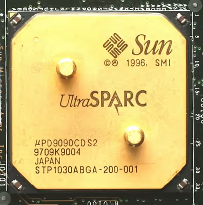
Commercial RISC designs began to emerge in the mid-1980s. The IBM RT PC was introduced in January 1986, and the Acorn ARM1 was introduced as part of an evaluation system in July 1986, following on from initial fabrication in April 1985. The MIPS R2000 was introduced in May 1986, followed shortly thereafter by Hewlett-Packard's PA-RISC in some of their computers. In the meantime, the Berkeley effort had become so well known that it eventually became the name for the entire concept. In 1987, Sun Microsystems began shipping systems with the SPARC processor, directly based on the Berkeley RISC-II system. The US government Committee on Innovations in Computing and Communications credits the acceptance of the viability of the RISC concept to the success of the SPARC system.
A benefit of RISC to the industry was much lower prices than the sole sourced Intel 80386; by 1989 many RISC CPUs were available, and competition lowered their price to $10 per MIPS in large quantities. The performance of IBM's RISC CPU—only available in the RT PC—was less competitive than others, but the success of SPARC renewed interest within IBM, which released new RISC systems by 1990 and by 1995 RISC processors were the foundation of a $15 billion server industry.
Patterson was a consultant for Intel during the 1980s. Despite dominating the microprocessor market with the CISC 80386 and its successors, the consensus that RISC was the future of the industry influenced that company's engineers, who worked to improve the performance of their processors to match RISC. IBM chose a similar approach of improving CISC as much as possible with IBM mainframes, while introducing new RISC-based computers that competed directly with its existing CISC midrange systems. Sun's move to SPARC was based on its decision to, instead of relying on improvements to CISC, transition to RISC as fast as possible. The DEC engineers who designed DECstation with MIPS R2000 and not their company's own VAX did so because, they wrote, the former offered "at least a two-to-one performance advantage" for the cost. By the later 1980s, new RISC designs were easily outperforming all CISC designs by a wide margin.
By 1992 Sun, DEC, HP, and IBM were the leading commercial RISC companies. Other vendors began their own RISC efforts. Among the available architectures were the DEC Alpha, AMD Am29000, Intel i860 and i960, Motorola 88000, IBM POWER, and, slightly later, the IBM/Apple/Motorola PowerPC. Many of these have since disappeared due to them often offering no competitive advantage over others of the same era. Those that remain are often used only in niche markets or as parts of other systems; of the designs from these traditional vendors, only SPARC and the PowerPC-derived Power ISA have any significant remaining market.
The ARM architecture has been the most widely adopted RISC ISA. It was initially intended to deliver higher-performance desktop computing at low cost and in a restricted thermal package, such as in the Acorn Archimedes, while featuring in the Super Computer League tables. Its initial relatively lower power and cooling implementation was soon adapted to embedded applications, such as laser printer raster image processing. In 1990, Acorn, Apple Inc and VLSI, created ARM Ltd, to share R&D costs and find new markets for the ISA, who in partnership with TI, GEC, Sharp, Nokia, Oracle and Digital would develop low-power and embedded RISC designs, and target those market segments, which at the time were niche. With the rise in mobile, automotive, streaming, smart device computing, ARM became the most widely used ISA. The company estimats that almost half of all CPUs shipped in history have been ARM.
Sign in to keep reading
4 more chapters are free with a Lably account.
Characteristics and design philosophy
Confusion around the definition of RISC deriving from the formulation of the term, along with the tendency to opportunistically categorize processor architectures with relatively few instructions (or groups of instructions) as RISC architectures, led to attempts to define RISC as a design philosophy. One attempt to do so was expressed as follows:
A RISC processor has an instruction set that is designed for efficient execution by a pipelined processor and for code generation by an optimizing compiler.
— Michael Slater, Microprocessor Report
Instruction set philosophy
A common misunderstanding of the phrase "reduced instruction set computer" is that instructions are simply eliminated, resulting in a smaller set of instructions. In fact, over the years, RISC instruction sets have grown in size, and today many of them have a larger set of instructions than many CISC CPUs. Some RISC processors such as the PowerPC have instruction sets as large as the CISC IBM System/370, for example; conversely, the DEC PDP-8—clearly a CISC CPU because many of its instructions involve multiple memory accesses—has only 8 basic instructions and a few extended instructions. The term "reduced" in that phrase was intended to describe the fact that the amount of work any single instruction accomplishes is reduced—at most a single data memory cycle—compared to the "complex instructions" of CISC CPUs that may require dozens of data memory cycles in order to execute a single instruction.
The term load–store architecture is sometimes preferred.
Another way of looking at the RISC/CISC debate is to consider what is exposed to the compiler. In a CISC processor, the hardware may internally use registers and flag bits in order to implement a single complex instruction such as STRING MOVE, but hide those details from the compiler. The internal operations of a RISC processor are "exposed to the compiler", leading to the backronym 'Relegate Interesting Stuff to the Compiler'.
Instruction format
Most RISC architectures have fixed-length instructions and a simple encoding, which simplifies fetch, decode, and issue logic considerably. This is among the main goals of the RISC approach.
Some of this is possible only due to the contemporary move to 32-bit formats. For instance, in a typical program, over 30% of all the numeric constants are either 0 or 1, 95% will fit in one byte, and 99% in a 16-bit value. When computers were based on 8- or 16-bit words, it would be difficult to have an immediate combined with the opcode in a single memory word, although certain instructions like increment and decrement did this implicitly by using a different opcode. In contrast, a 32-bit machine has ample room to encode an immediate value, and doing so avoids the need to do a second memory read to pick up the value. This is why many RISC processors allow a 12- or 13-bit constant to be encoded directly into the instruction word.
Assuming a 13-bit constant area, as is the case in the MIPS and RISC designs, another 19 bits are available for the instruction encoding. This leaves ample room to indicate both the opcode and one or two registers. Register-to-register operations, mostly math and logic, require enough bits to encode the two or three registers being used. Most processors use the three-operand format A = B + C, in which case three register numbers are needed. If the processor has 32 registers, each one requires a 5-bit number for 15 bits total. If one of these registers is replaced by an immediate, there is still room to encode the two remaining registers and the opcode. Common instructions found in multi-word systems, like INC and DEC, which reduce the number of words that have to be read before performing the instruction, are unnecessary in RISC as they can be accomplished with a single register and the immediate value 1.
The original RISC-I format remains a canonical example of the concept. It uses 7 bits for the opcode and a 1-bit flag for conditional codes, the following 5 bits for the destination register, and the next five for the first operand. This leaves 14 bits, the first of which indicates whether the following 13 contain an immediate value or use only five of them to indicate a register for the second operand. A more complex example is the MIPS encoding, which uses only 6 bits for the opcode, followed by two 5-bit registers. The remaining 16 bits could be used in two ways: one as a 16-bit immediate value, or as a 5-bit shift value (used only in shift operations, otherwise zero) and the remaining 6 bits as an extension on the opcode. In the case of register-to-register arithmetic operations, the opcode was 0 and the last 6 bits contained the actual code; those that used an immediate value used the normal opcode field at the front.
One drawback of 32-bit instructions is reduced code density, which is a more adverse characteristic in embedded computing than it is in the workstation and server markets that RISC architectures were originally designed to serve. To address this problem, several architectures, such as SuperH (1992), ARM thumb (1994), MIPS16e (2004), Power Variable Length Encoding ISA (2006), RISC-V, and the Adapteva Epiphany, have an optional short, feature-reduced compressed instruction set. Generally, these instructions expose a smaller number of registers and fewer bits for immediate values, and often use a two-operand format to eliminate one register number from instructions. A two-operand format in a system with 16 registers requires 8 bits for register numbers, leaving another 8 for an opcode or other uses. The SH5 also follows this pattern, albeit having evolved in the opposite direction, having added longer 32-bit instructions to an original 16-bit encoding.
Hardware utilization
The most characteristic aspect of RISC is executing at least one instruction per cycle. Single-cycle operation is described as "the rapid execution of simple functions that dominate a computer's instruction stream", thus seeking to deliver an average throughput approaching one instruction per cycle for any single instruction stream.
Other features of RISC architectures include:
- Far fewer transistors are dedicated to the core logic, which originally allowed designers to increase the size of the register set and increase internal parallelism.
- Uniform instruction format, using a single word with the opcode in the same bit positions for simpler decoding
- All general-purpose registers can be used equally as source/destination in all instructions, simplifying compiler design (floating-point registers are often kept separate)
- Simple addressing modes with complex addressing performed by instruction sequences
- Few data types in hardware (no byte string or binary-coded decimal [BCD], for example)
RISC designs are also more likely to feature a Harvard memory model, where the instruction stream and the data stream are conceptually separated; this means that modifying the memory where code is held might not have any effect on the instructions executed by the processor (because the CPU has a separate instruction and data cache), at least until a special synchronization instruction is issued; CISC processors that have separate instruction and data caches generally keep them synchronized automatically, for backwards compatibility with older processors.
Many early RISC designs also shared the characteristic of having a branch delay slot, an instruction space immediately following a jump or branch. The instruction in this space is executed, whether or not the branch is taken (in other words, the effect of the branch is delayed). This instruction keeps the ALU of the CPU busy for the extra time normally needed to perform a branch. Nowadays, the branch delay slot is considered an unfortunate side effect of a particular strategy for implementing some RISC designs, and modern RISC designs generally do away with it (such as PowerPC and more recent versions of SPARC and MIPS).
Some aspects attributed to the first RISC-labeled designs around 1975 include the observations that the memory-restricted compilers of the time were often unable to take advantage of features intended to facilitate manual assembly coding, and that complex addressing modes take many cycles to perform due to the required additional memory accesses. It was argued that such functions would be better performed by sequences of simpler instructions if this could yield implementations small enough to leave room for many registers, reducing the number of slow memory accesses. In these simple designs, most instructions are of uniform length and similar structure; arithmetic operations are restricted to CPU registers and only separate load and store instructions access memory. These properties enable a better balancing of pipeline stages than before, making RISC pipelines significantly more efficient and allowing higher clock frequencies.
Yet another impetus for both RISC and other designs came from practical measurements on real-world programs. Andrew Tanenbaum summed up many of these, demonstrating that processors often had oversized immediates. For instance, he showed that 98% of all the constants in a program would fit in 13 bits, yet many CPU designs dedicated 16 or 32 bits to store them. This suggests that, to reduce the number of memory accesses, a fixed-length machine could store constants in unused bits of the instruction word itself, so that they would be immediately ready when the CPU needs them (much like immediate addressing in a conventional design). This required small opcodes in order to leave room for a reasonably sized constant in a 32-bit instruction word.
Since many real-world programs spend most of their time executing simple operations, some researchers decided to focus on making those operations as fast as possible. The clock rate of a CPU is limited by the time it takes to execute the slowest sub-operation of any instruction; decreasing that cycle time often accelerates the execution of other instructions. The focus on "reduced instructions" led to the resulting machine being called a "reduced instruction set computer" (RISC). The goal was to make instructions so simple that they could easily be pipelined, in order to achieve a single clock throughput at high frequencies. This contrasted with CISC designs whose "crucial arithmetic operations and register transfers" were considered difficult to pipeline.
Later, it was noted that one of the most significant characteristics of RISC processors was that external memory was only accessible by a load or store instruction. All other instructions were limited to internal registers. This simplified many aspects of processor design: allowing instructions to be fixed-length, simplifying pipelines, and isolating the logic for dealing with the delay in completing a memory access (cache miss, etc.) to only two instructions. This led to RISC designs being referred to as load–store architectures.
Comparison to other architectures
Some CPUs have been specifically designed to have a very small set of instructions—but these designs are very different from classic RISC designs, so they have been given other names such as minimal instruction set computer (MISC) or transport triggered architecture (TTA).
RISC architectures have traditionally had few successes in the desktop PC and commodity server markets, where the x86-based platforms remain the dominant processor architecture. However, this may change, as ARM-based processors are being developed for higher-performance systems. Manufacturers including Cavium, AMD, and Qualcomm have released server processors based on the ARM architecture. ARM further partnered with Cray in 2017 to produce an ARM-based supercomputer. On the desktop, Microsoft announced that it planned to support the PC version of Windows 10 on Qualcomm Snapdragon-based devices in 2017 as part of its partnership with Qualcomm. These devices will support Windows applications compiled for 32-bit x86 via an x86 processor emulator that translates 32-bit x86 code to ARM64 code. Apple announced they will transition their Mac desktop and laptop computers from Intel processors to internally developed ARM64-based SoCs called Apple silicon; the first such computers, using the Apple M1 processor, were released in November 2020. Macs with Apple silicon can run x86-64 binaries with Rosetta 2, an x86-64 to ARM64 translator.
Outside of the desktop arena, however, the ARM RISC architecture is in widespread use in smartphones, tablets and many forms of embedded devices. While early RISC designs differed significantly from contemporary CISC designs, by 2000 the highest-performing CPUs in the RISC line were almost indistinguishable from the highest-performing CPUs in the CISC line.
Use of RISC architectures
RISC architectures are now used across a range of platforms, from smartphones and tablet computers to some of the world's fastest supercomputers such as LineShine, El Capitan, and Frontier, the top 3 fastest on the TOP500 list as of June 2026.
Low-end and mobile systems
By the beginning of the 21st century, the majority of low-end and mobile systems relied on RISC architectures. Examples include:
- The ARM architecture dominates the market for low-power and low-cost embedded systems (typically 200–1800 MHz in 2014). It is used in a number of systems such as most Android-based systems, the Apple iPhone, iPod Touch, iPad, Apple Watch, and Apple TV, Palm, Microsoft Windows Phone (former Windows Mobile / Windows CE), RIM devices, Nintendo Game Boy Advance, DS, 3DS and Switch, Raspberry Pi, etc.
- IBM's PowerPC was used in the GameCube, Wii, PlayStation 3, Xbox 360 and Wii U gaming consoles.
- The MIPS line (at one point used in many SGI computers) was used in the PlayStation, PlayStation 2, Nintendo 64, PlayStation Portable game consoles, and residential gateways like Linksys WRT54G series.
- Hitachi's SuperH, originally in wide use in the 32X, Saturn, and Dreamcast consoles, now developed and sold by Renesas as the SH4.
- Atmel AVR, used in a variety of products ranging from Xbox handheld controllers and the Arduino open-source microcontroller platform to BMW cars.
- RISC-V, the current iteration of Berkeley's open standard RISC ISA, with 32- or 64-bit address spaces, a small core integer instruction set, and an experimental "Compressed" ISA for code density and designed for standard and special-purpose extensions.
Desktop and laptop computers
- IBM's PowerPC architecture was used in Apple's Macintosh computers from 1994, when they began a switch from Motorola 68000 family processors, to 2005, when they transitioned to Intel x86 processors.
- Some Chromebooks use ARM-based platforms since 2012.
- Apple uses inhouse-designed processors based on the ARM architecture for its lineup of desktop and laptop computers since its transition from Intel processors, and the first such computers were released in November 2020.
- Microsoft uses Qualcomm ARM-based processors for its Surface line. HP Inc and Lenovo have released Windows PCs with an ARM-based Qualcomm Snapdragon.
Workstations, servers, and supercomputers
- MIPS, by Silicon Graphics (ceased making MIPS-based systems in 2006).
- SPARC, by Oracle (previously Sun Microsystems), and Fujitsu.
- IBM's IBM POWER architecture, PowerPC, and Power ISA were and are used in many of IBM's supercomputers, mid-range servers and workstations.
- Hewlett-Packard's PA-RISC, also known as HP-PA (discontinued at the end of 2008).
- Alpha, used in single-board computers, workstations, servers and supercomputers from Digital Equipment Corporation, then Compaq and finally Hewlett-Packard (HP)(discontinued as of 2007).
- RISC-V, the fifth Berkeley RISC ISA, with 64- or 128-bit address spaces, and the integer core extended with floating point, atomics and vector processing, and designed to be extended with instructions for networking, I/O, and data processing. A specification for a 64-bit superscalar design, "Rocket", is available for download. It is implemented in the European Processor Initiative processor.
- The ARM architecture currently in use by cloud providers for servers. One example is the AWS Graviton series processor used for various services on the AWS platform. ARM was also used in the Fujitsu A64FX chip to create Fugaku, the world's fastest supercomputer in 2020.
Open source, standard, or use
RISC architectures have become popular in open source processors and soft microprocessors since they are relatively simple to implement, which makes them suitable for FPGA implementations and prototyping, for instance. Examples include:
- OpenRISC, an open instruction set and micro-architecture first introduced in 2000.
- Open MIPS architecture, for part of 2019, the specifications were free to use, royalty free, for registered MIPS developers.
- OpenSPARC, in 2005, Sun released its Ultra Sparc documentation and specifications under the GPLv2.
- LEON, an open source, radiation-tolerant implementation of the SPARC V8 instruction set (targeting space applications).
- Libre-SOC, an open source SoC based on the Power ISA with extensions for video and 3D graphics.
- RISC-V, in 2010, the Berkeley RISC version 5, specification, tool chain, and brand, were made available, free of charge, for non-commercial purposes.
- SuperH - J Core, in 2015, a project to offer clean room implementations of the patent-expired Hitachi SuperH RISC ISA was started.
- ARM DesignStart, in 2018, ARM, in partnership with FPGA supplier Xilinx, started to offer free access to some of ARM's IP, including FPGA specifications for some older CPU cores.
Awards
In 2022 Steve Furber, John L. Hennessy, David A. Patterson and Sophie M. Wilson were awarded the Charles Stark Draper Prize by the United States National Academy of Engineering for their contributions to the invention, development, and implementation of reduced instruction set computer (RISC) chips.